Electromagnetic Fields
in Printed Circuit Boards
An interactive visual guide to understanding how electromagnetic fields behave in PCBs — from a single conductor to the complete two-conductor system that underpins all EMC design.

Before understanding EMI in PCBs, you must understand what a single conductor does to the surrounding space. Every EMI problem traces back to what happens when these fields are not properly contained.
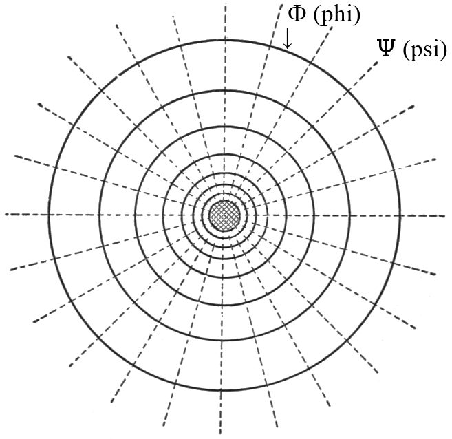
Figure 1 - Electric Field of Conductor.
Key observation: With a single conductor, the electric field lines radiate outward to infinity. There is no containment. This is exactly what happens when a PCB trace has no adjacent Return Reference Plane — the fields spread uncontrolled into free space.
Closed Loops — Always
Magnetic field lines always form closed loops. They encircle the conductor, forming what can be described as a magnetic circuit. The field strength decreases with distance from the conductor.
Radiate Outward
Around a single conductor, electric field lines radiate outward as straight lines. They have no termination point — they spread to infinity. This is an uncontained field — a radiating antenna.
Introducing a second conductor — the return — transforms the field geometry entirely. Electric field lines now terminate at the second conductor instead of radiating to infinity. Magnetic field lines concentrate in the space between. This is the foundation of EMI control.
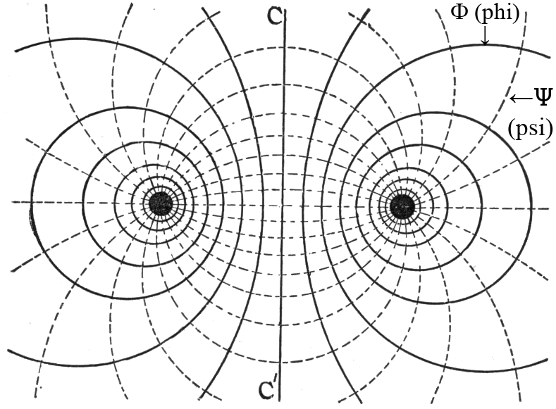
Figure 2 - Electric and magnetic fields around the conductors in a circuit.
The transformation: Adding the return conductor changes everything. Magnetic field lines become concentrated loops in the space between conductors. Electric field lines now originate from one conductor and terminate at the other — they no longer radiate to infinity. This is field containment.
Concentrated Between Conductors
Instead of concentric circles expanding to infinity, the magnetic field now forms stronger, more focused loops concentrated in the space between the two conductors. Outside this space, the field drops away rapidly.
Terminate at the Return
Electric field lines now originate from the signal conductor and terminate at the return conductor. This is the key — they no longer radiate outward. The return conductor provides the reference that contains the field.
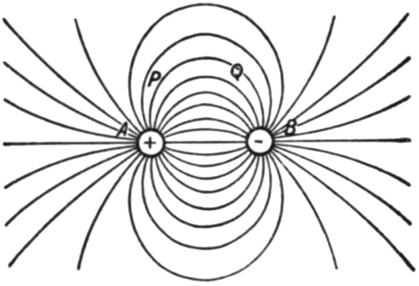
Figure 3 - Electric bodies with equal but opposite charges.
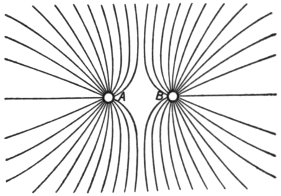
Figure 4 - Electric bodies with equal charge.
Think of the two conductors as riverbanks — they don't carry the water, they contain and direct it. In PCB design, the trace and reference plane are the riverbanks, and the electromagnetic fields are the river flowing in between. Your job as a designer is to engineer these riverbanks, not the current in the copper.
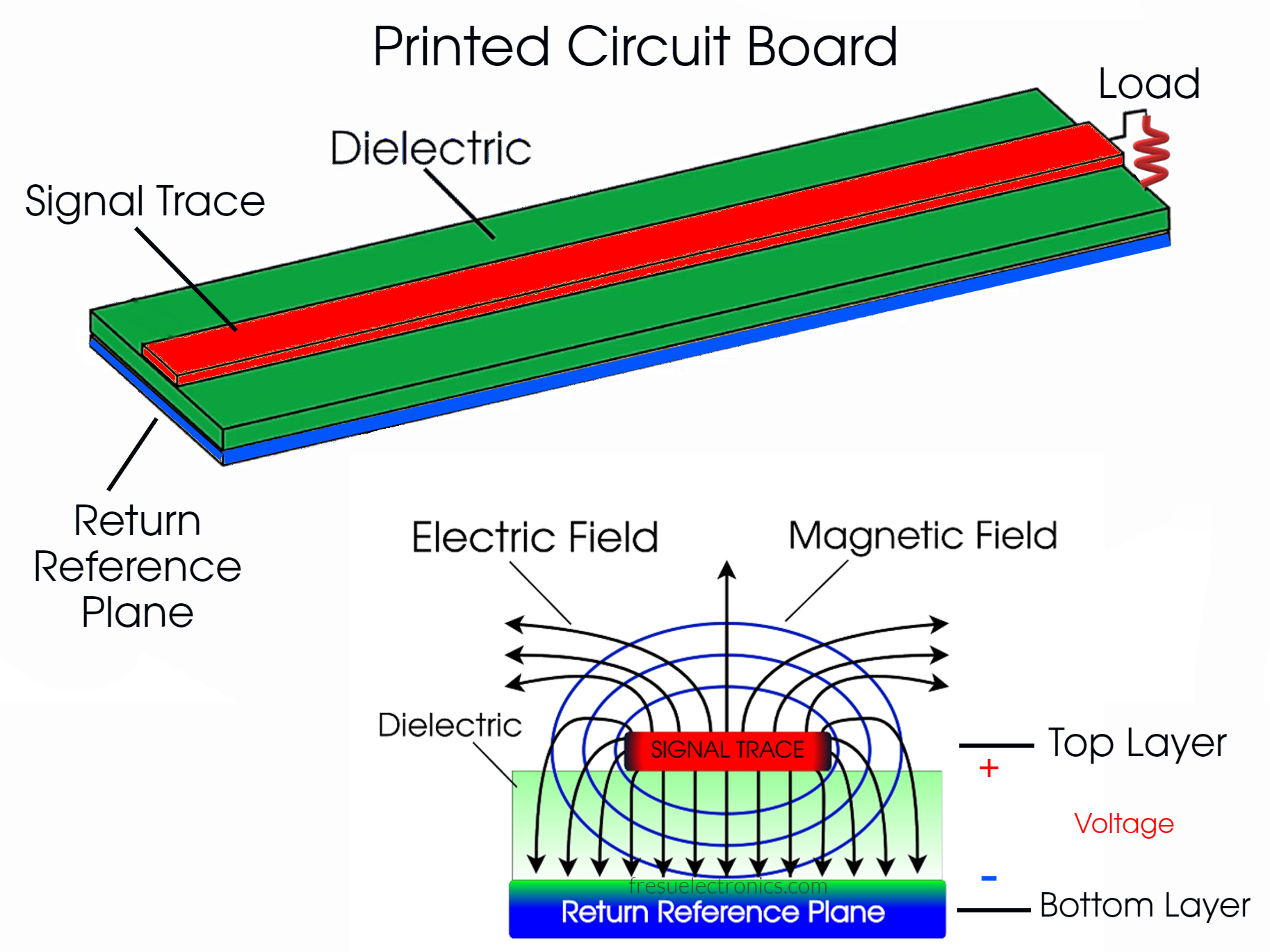
Figure 5 - Electric and Magnetic Field in a PCB.
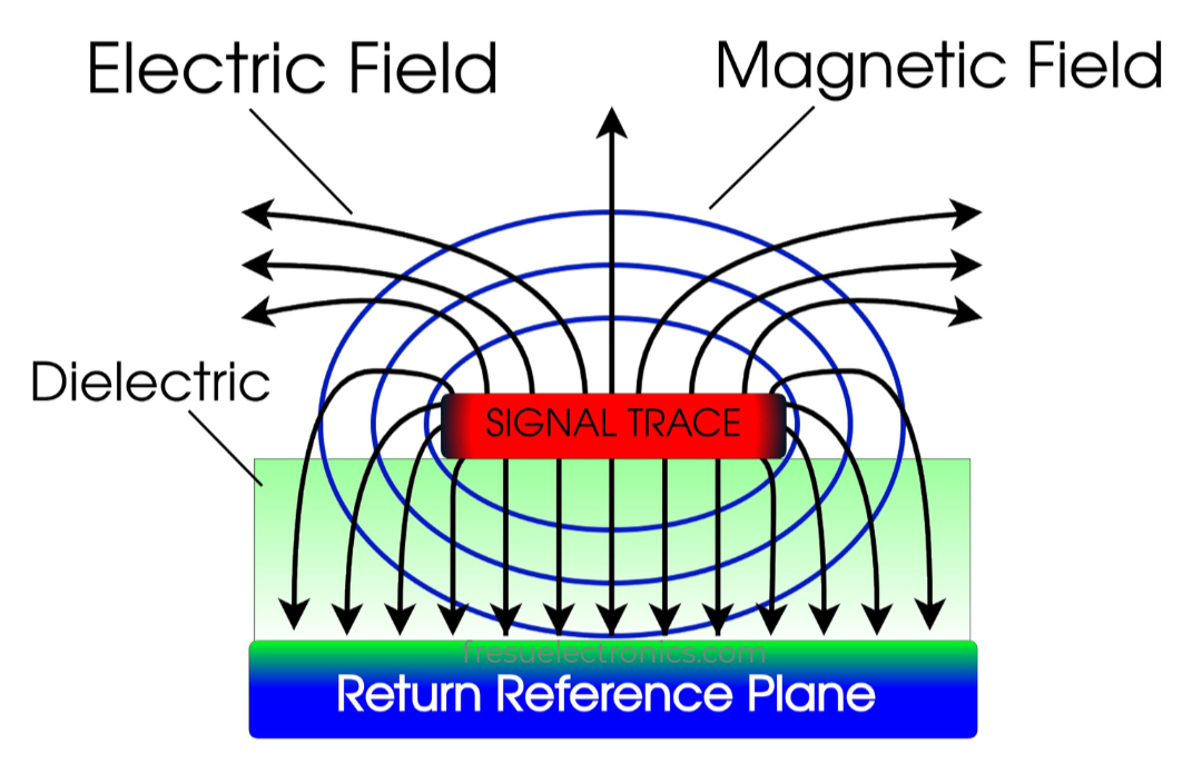
Figure 6 - Electric and Magnetic Field in a PCB, cross-section view.
The rotation insight: The PCB trace + RRP is exactly the same as the two-conductor system — just rotated 90°. The signal trace is one riverbank. The RRP is the other. The FR4 dielectric between them is where the electromagnetic energy actually propagates. The dielectric is more important than the conductors themselves.
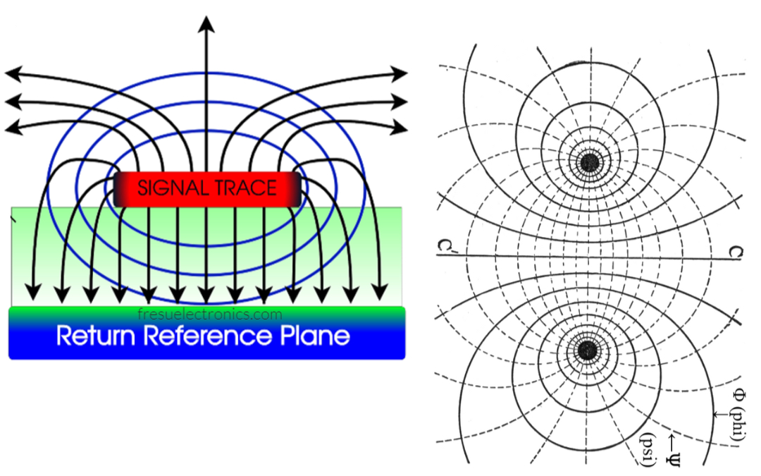
Figure 7 - Electric and Magnetic Field in a PCB in compared to two wires topology.
More Important Than the Copper
The copper guides the fields, but the energy propagates in the FR4 dielectric. When you choose a stackup, you are choosing the medium in which your signal energy travels. FR4 is one of the lossiest common dielectrics — important at high frequencies.
Direction of Energy Flow
The Poynting vector (S = E × H) describes the direction electromagnetic energy propagates. It points along the trace — into the page in this view. Energy moves between the conductors, not through them.
Energy is described as electrons flowing through the copper conductor from source to load. The ground wire carries them back. This model explains Ohm's law and DC circuits — nothing more.
Why it fails: It cannot explain why signals travel at ~half the speed of light. It cannot explain EMI or radiation. It cannot explain why a nearby ground plane reduces emissions.
Energy propagates as electromagnetic fields in the dielectric space between conductors. The conductors are boundaries that steer the fields. The Poynting vector describes the direction of energy flow.
Why it matters: This model explains everything the electron model cannot — radiation, field containment, why the RRP matters, why splits cause EMI, and how to design for low emissions.
For every signal layer, there must be a Return Reference Plane adjacent to it. That plane must be solid and continuous — free of holes, cuts, gaps, or splits. Without this, the PCB is a radiating antenna, not a controlled transmission system. This single rule is responsible for more EMC pass/fail outcomes than any other design decision.
Figure 8 - Electric and Magnetic Field in a PCB, cross-section view.
Fields Contained — Low EMI
Fields confined to the dielectric. Return current flows directly under the trace. Minimum loop area, minimum inductance, minimum radiation. This is the target in every design.
PCB Becomes a Radiator
Fields expand outward until they find the earth ground. Common mode currents form along the large loop area. Radiated emissions are easily 20–40 dB higher. First EMC test failure cause.
Return Current Forced Around Gap
A plane split forces return current to detour, creating a large current loop — an efficient antenna structure. Splitting planes to "separate" analog and digital domains does not help EMI — it causes it.
Fragmented Copper Is Not a Plane
Adding copper pour is not the same as a proper RRP. Fragmented, disconnected patches create antenna-like structures that generate additional common-mode noise. A proper RRP must be solid and continuous.

Figure 9 - Electric and Magnetic fields in a two layers PCB.