

This article will walk you through the fundamentals of performing an EMI project review for a Printed Circuit Board layout. We'll concentrate on a motherboard design that includes AllWinner-A64 processors, which is a fairly intricate system.
The project under review is the TERES-I from Olimex. As EMI specialists, we will examine the key areas to focus on to enhance the board's EMI performance.
WATCH THE LESSON HERE:
PCB Layer Arrangement
One of the first things I check during an EMI review is whether the stackup is correct.
Getting the stackup right accounts for about 90% of the EMI performance.
Why is that?
Because the stackup determines how the electromagnetic fields are contained within the PCB.
What do I mean by that?
In PCB design, layers always come in pairs.
For example, if I have a signal layer, there must automatically be a return reference plane (RRP) adjacent to it—this should be second nature.
What does "adjacent" mean?
It means the return reference plane should be directly above or below the signal layer.
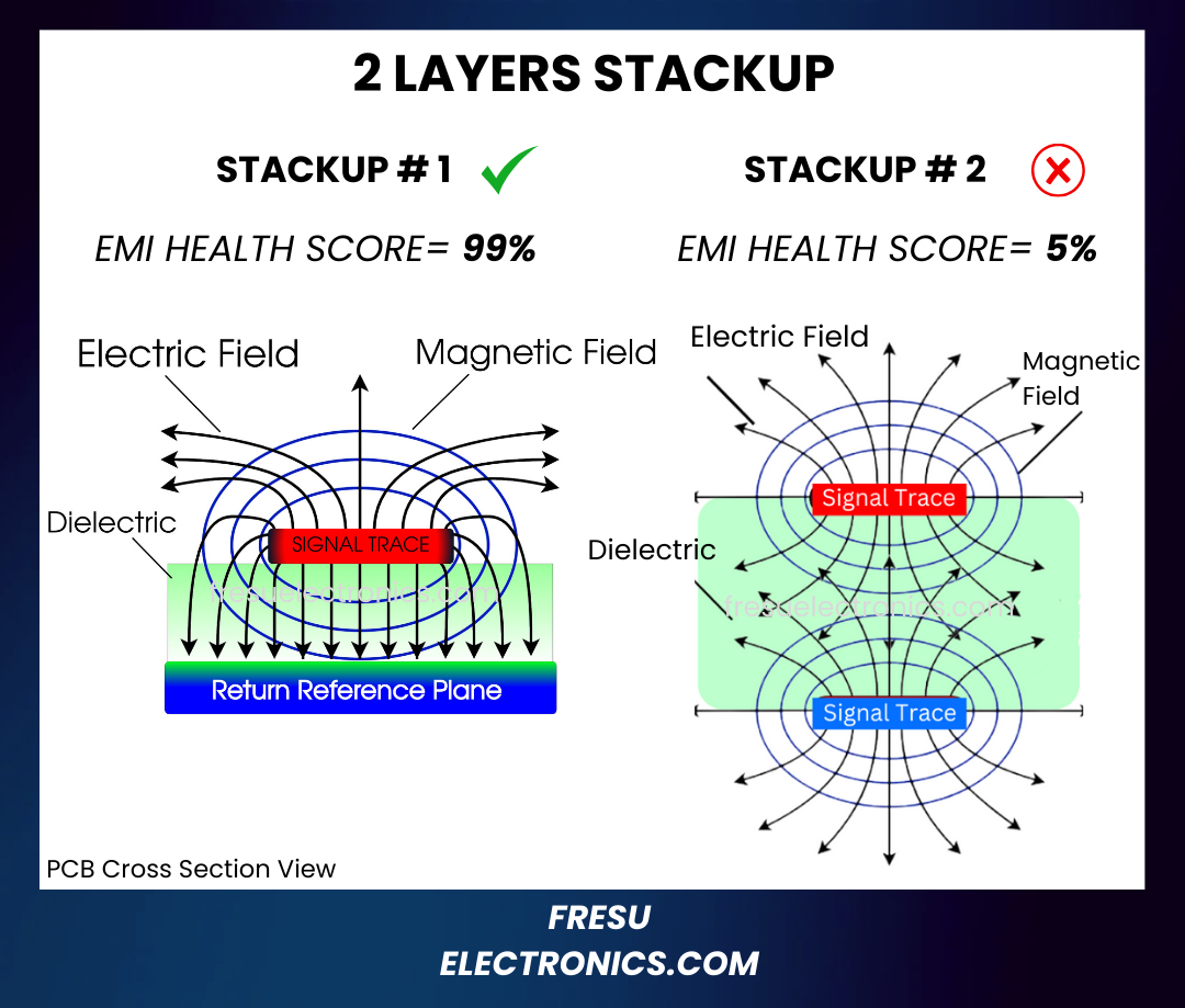
Figure 1 - Comparison between 2 layers PCB stackup
It’s important that the return reference plane (RRP) is placed as close as possible to the signal layer to do its job effectively.
As the name suggests, the RRP provides the return path for the current to flow back to its source, and it also offers a reference potential for the signal layer.
If this setup is not in place, we are likely to face EMI issues as well as signal integrity problems. This is because, without proper containment, the electromagnetic fields can "spread out" rather than being confined by the stackup.
When the RRP is placed as close as possible to the signal layer, the electromagnetic fields remain "smaller" and more controlled.
One key point to highlight is that the power layer does not work well as a return reference plane.
This is because, for the return current to flow back to its source, it would need to cross multiple layers before finally closing the loop and reaching the source pin. This leads to poor EMI performance and signal integrity.
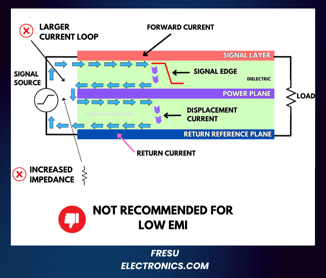
Figure 2 - Example of a Power plane used instead of a RRP.
What does this mean?
It means that the return current must travel through the space between the layers, which has its own impedance. As the current flows through this space, it creates a voltage drop that introduces noise within the stackup.
This noise can lead to crosstalk between signals on adjacent layers and may even cause emissions from the edges of the board.
For this reason, I do not recommend using the power plane as a return path, especially for high-speed signals.
You might have heard suggestions about using stitching capacitors, but the issue is that the impedance of these capacitors at high frequencies tends to be inductive.
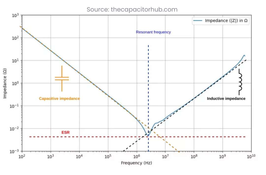
Figure 3 - Example of the capacitor Impedance
This means that the high-frequency portion of the return current will not flow through the decoupling capacitor; instead, it will travel through the layers as displacement current.
As a result, this displacement current will spread between the layers, seeking the path of least impedance to return to the source and complete the current loop.
In contrast, the low-frequency portion of the current flowing through the decoupling capacitor often takes a larger loop, which can create common mode currents that lead to emissions.
For these reasons, we should avoid using the power layer as a return layer.
At least, I no longer do!
Optimal 6 Layers Stackup
We can immediately see that the stackup is composed of 6 layers.
Figure 4 - PCB Stackup of the board.
I expect to see at least two Return Reference Planes (RRP) because each signal should have an RRP adjacent to it, or at least on one side where it couples.
There are several ways this stackup can work effectively, particularly in terms of EMI and signal integrity.
Stackup Option 1
One option is to have Layer 1 dedicated to signals and power, paired with the RRP on Layer 2. Layer 3 can also have signals and power, paired with the RRP on Layer 2. The remaining layers, Layers 4, 5, and 6, would mirror the first three layers.
This configuration means Layer 4 will have signals and power paired with Layer 5 as the full RRP, and Layer 6 will also be paired with the RRP on Layer 5.
We can achieve this due to the skin depth effect, which allows return currents from Layers 1 and 3 to reside on Layer 2 without mixing. The return current from Layer 1 occupies one side of Layer 2, while the return current from Layer 3 occupies the opposite side.
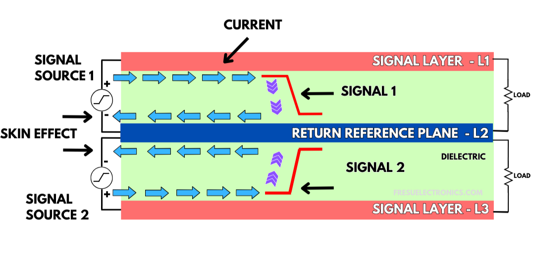
Figure 5 - Skin depth effect in the PCB stackup.
This arrangement ensures that the skin depth calculated for the signals permits two different return currents without causing crosstalk.
The same principle applies to Layer 5, which serves as the RRP for both Layers 4 and 6.
When I refer to signals and power, I mean routed with tracks rather than as planes or large copper pours.
With this stackup, we effectively utilize four layers for signals and power, potentially creating a more cost-effective design. However, we must be cautious that Layers 3 and 4 do not interfere with each other, making a thicker dielectric layer between them advisable.
Stackup Option 2
Another effective stackup option is to pair Layer 1 as signals with Layer 2 as the RRP. Similarly, Layer 6 can serve as signals paired with Layer 5 as the RRP.
In this setup, Layers 3 and 4 can be dedicated power planes, increasing the amount of current we can deliver.
Stackup Option 3 - Mixed
A mixed option combines the two approaches I just proposed. In this setup, Layers 1 and 6 are used for signals and power, while Layers 2 and 5 serve as RRPs. Layers 3 and 4 can be used interchangeably as signals or power planes.
They do not need to be of the same type; for example, Layer 3 can be a signal layer while Layer 4 can be a power plane.
These configurations represent some of the most effective combinations for a six-layer stackup.
As a general rule, always think in terms of assigning layers in pairs, not as individual layers. Each pair should consist of signals and RRPs or power and RRPs.
In any case, an RRP must be present. Any deviation from this structure can create antenna-like behaviors and result in poor EMI performance, as the electromagnetic fields will begin to spread.
Analysis of the Current Board Stackup
Now, we will examine the layer arrangement and conduct an analysis to ensure that the stackup does not introduce potential EMI issues.
The first layer is dedicated to components and signal routing, along with some power distribution.
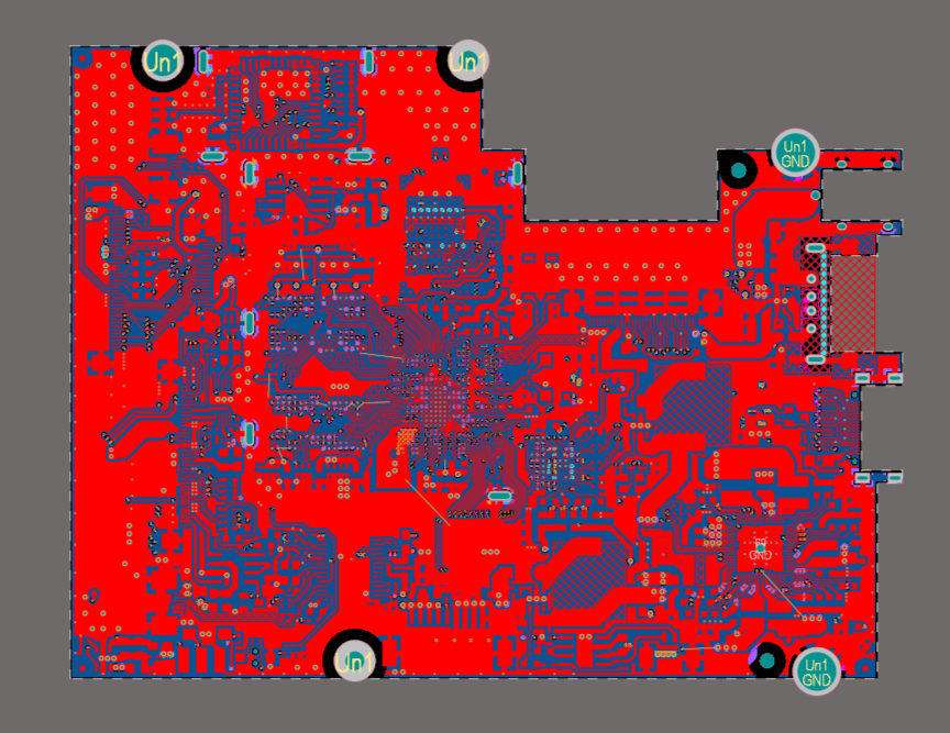
Figure 6 - Layer 1
This is a typical choice.
As mentioned earlier, the second layer should serve as the Return Reference Plane (RRP).
Let's take a look at what has been implemented here.
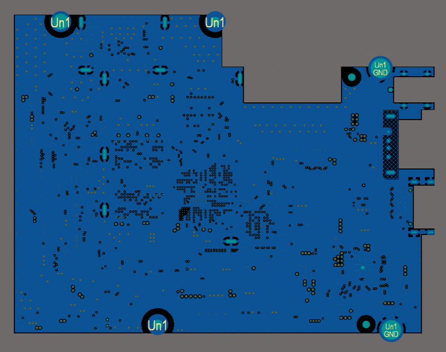
Figure 7 - Layer 2
Great! This aligns perfectly with our expectations.
With this configuration, we have a complete pair for Layers 1 and 2.
Notice how the second layer is a solid plane without splits, cuts, or large gaps. This ensures that the signals on Layer 1 always have an RRP directly underneath throughout their entire propagation.
By examining any trace on the board and verifying that there’s a good RRP beneath it, you can avoid impedance discontinuities. This is crucial for maintaining a consistent signal and preventing issues like reflections or unwanted emissions that can occur when impedance changes.
Now, let’s take a look at Layer 3.
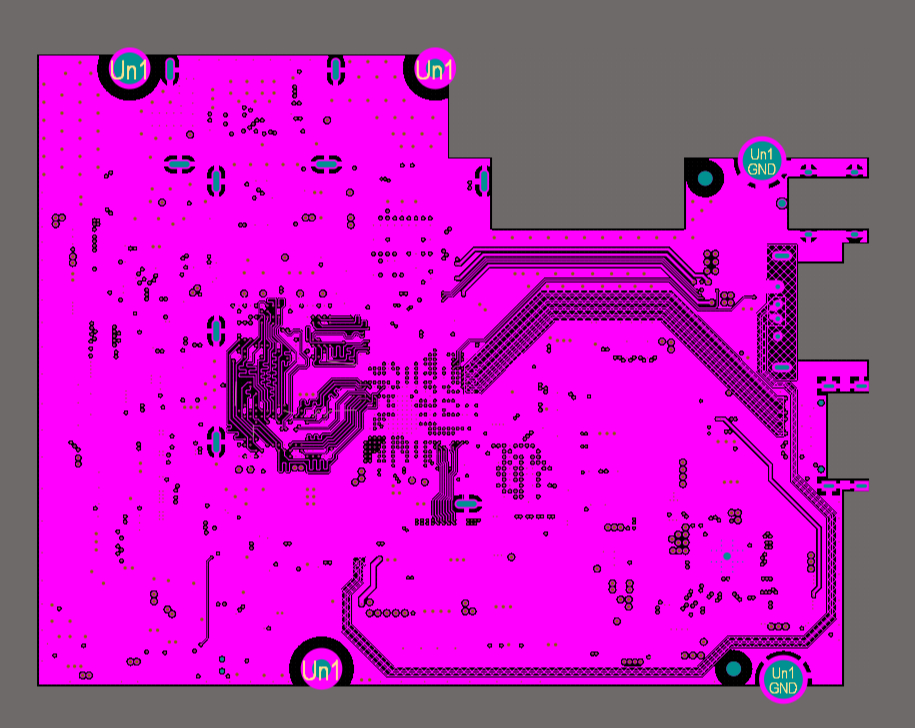
Figure 8 - Layer 3
This layer is also a plane, but this time it includes some digital signals.
This is still a good configuration, as the signals on Layer 3 are paired with the RRP on Layer 2.
Now, let’s examine Layer 4.
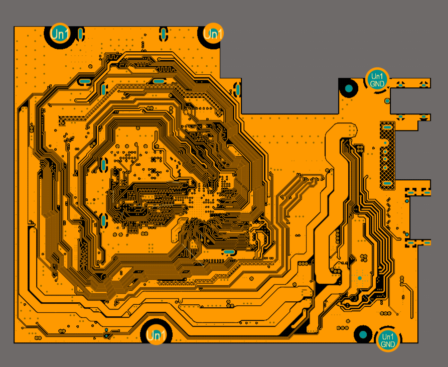
Figure 9 - Layer 4
This is where most of the routing has been done, featuring many digital and power signals. Additionally, there are large sections of copper connected to the ground (GND) net.
So far, so good.
As I mentioned earlier, I expect Layer 5 to serve as another RRP, which should pair with the signals on Layer 4.
Let’s see what has been chosen for this layer.
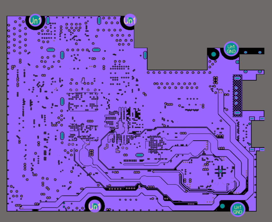
Figure 10 - Layer 5
Here, we have a mixed power layer.
There is a large copper area for the 3.3V supply, along with other voltages represented by traces or polygon fills.
This configuration may lead to issues for us.
Now, let’s examine the last layer, Layer 6.
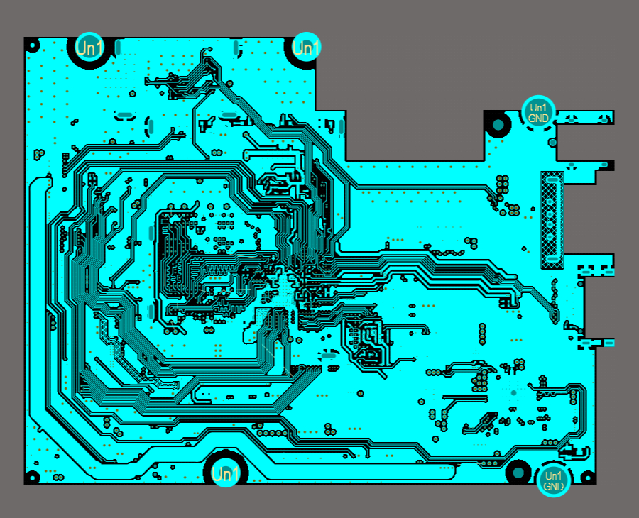
Figure 11 - Layer 6
This layer is dedicated to digital signals and power, and it includes a large copper area for the ground (GND) net.
Now, let me explain the issues with having the power layer on Layer 5.
There are two main problems that arise from this configuration, which makes this plane unsuitable for providing the return path for the currents from Layers 4 and 6:
- Impedance Discontinuity:
First, we have signals crossing splits horizontally. This results in parts of the signals lacking a plane beneath them, leading to impedance discontinuity.
This means that when the signal reaches the split, its impedance changes, resulting in signal variations and reflections.
- Return Current Path: The return current from Layers 4 and 6 now flows in Layer 5, but it still needs to return to the source to close the current loop.
Since Layer 5 is not connected to Layer 2 (the reference plane and zero-volt potential for the signal), the return current must find a way to travel from Layer 5 to Layer 2.
However, there is no DC connection between the two layers. Remember, Layer 2 is the GND net, while Layer 5 is a power layer.
If there were a DC connection between them, it would create a short circuit! Thus, the return current relies on capacitance between these two planes.
This connection occurs either through decoupling capacitors between Layer 5 and Layer 2 or through the internal capacitance between the layers, which means the return current travels as displacement current.
As mentioned earlier, the challenge with conduction current flowing through the capacitors is that their impedance remains low only up to the resonant frequency. Beyond this frequency, the capacitor’s impedance becomes increasingly inductive.
The low-frequency portion of the current flowing through these capacitors will create larger current loops, which can generate common mode voltage sources, a significant concern for emissions.
The high-frequency component of the current that must return to the source, traveling as displacement current, must flow through the dielectric between the layers. This causes it to spread in search of the path of least impedance to reach the source.
As it crosses the dielectric, this material also possesses impedance; otherwise, we wouldn't observe any current flow.
As the current flows through this impedance, it generates a voltage drop across the layers. This voltage drop manifests as noise between the layers, which can also lead to emissions from the edges of the board.
Consequently, this can result in EMI issues and signal integrity problems, as this noise couples with other signals transitioning from one layer to another via vias.
This is why, as mentioned previously, we avoid using the power plane to provide the return current for signals. The only acceptable pairs are SGN-RRP and PWR-RRP, where RRP is the reference plane.
I wouldn't recommend any other combinations unless we intentionally want to create radiators! Therefore, the stackup should be changed to one of the versions I previously described in order to maintain a 6-layer board.
However, this modification would require changing the entire layout of the board. At this point, we can discuss with the client what actions can be taken and which options are available based on the project timeline. This highlights the importance of understanding the impact of EMI before we even start laying out the board.
Another option is to introduce additional return reference planes to meet the requirements of the signals and power layers. However, this would mean increasing the stackup by at least two more layers, resulting in an 8-layer board.
In summary, we have two options:
Option 1: Keep the 6-layer configuration but re-route the board to ensure that Layer 5 serves as a Return Reference Plane.
Option 2: Add two more layers, ideally with two more return reference planes, resulting in an 8-layer board.
Option 1 is the more time-consuming choice, as it requires a layout rework, which entails additional engineering costs. However, if executed correctly, this option allows us to maintain a 6-layer board with the expected production costs.
Option 2 is faster because it likely requires only minor modifications to the layout at this stage while still ensuring a solid stackup from an EMI perspective. However, this option may increase the cost of the stackup, so we need to account for this during production.
In this case, we can place an RRP between Layers 5 and 6 to provide a return path for both. I would also position another RRP between Layers 5 and 4, ensuring a close RRP for Layer 4, which primarily carries digital signals.
Our task will be to present this information to our clients or project stakeholders, especially if we are working for a company.
Layout Analysis
Now that we have reviewed the stackup, let's take a look at the layout itself.
At this point, we want to ensure that there are no visible issues or anomalies in the layout.
💡 By the way, If you would like to master EMC/EMI design, we have a new training program here:
There, you’ll find details on how to apply for one of our exclusive programs designed to help you achieve that goal.
Antenna-like Structures
The first thing we are going to check is for antenna-like structures.
I can already see something I'm not particularly fond of: the way some copper pours have been used.
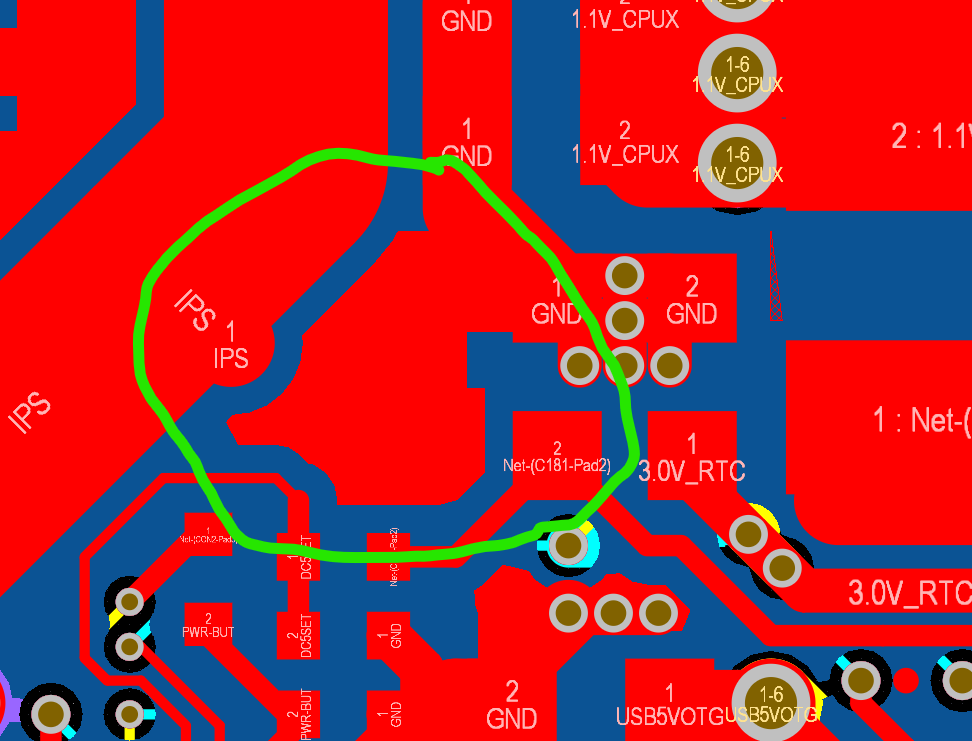
Figure 12 - Example of an antenna-like structure
This is concerning because these structures can create emissions problems.
What do I mean by antenna-like structures?
For example:
- Floating Copper Islands:
If there are copper areas that are not properly connected or not connected at all, they can act as small antennas. These floating patches can pick up or radiate signals, leading to EMI. Even if they are connected but not sufficiently, these portions of copper fills will still behave like antenna structures. Depending on the frequency of the signals that couple to them, voltage drops can occur through the parasitics of the copper fill, causing them to radiate.
- Long, Thin Traces with No Return Path:
When these traces extend over long distances without a nearby return reference plane, they can behave like dipole antennas, radiating energy into the environment.
- Unconnected Stubs or Branches:
Sometimes, designers leave unused portions of copper or traces branching off signal lines. These stubs can reflect signals and radiate them, acting like antennas.
- Presence of Slots or Gaps in the Return Reference Plane:
We've covered this during the stackup analysis, so we won’t elaborate further. We will ensure this issue is resolved by selecting the appropriate stackup proposed earlier.
In general, when conducting the EMI review, and most importantly, during the layout of the board, we must consider electromagnetic fields and frequencies.
It’s essential to understand how the parasitic behavior of the layout changes with signal frequency and its harmonics.
Layer 1 Review
Let’s start with layer 1.
1. Remove Copper Pours:
The first thing I recommend is to eliminate these copper pours.
Before making any modifications, ensure you have a copy of the project, as I do in this case.
Removing the copper fill will help get rid of the antenna-like structures I mentioned earlier. It will also allow us to check if the net used for the return current and reference, typically the GND, has all its pins and connections made with the lowest possible inductance.
2. Optimize GND Vias:
I want to assess if the GND vias are placed as close as possible to the component pads. This placement reduces the inductance of the return path because the current will be much closer to the return reference plane (RRP).
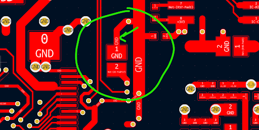
Figure 13 - Example of missing vias per each GND pad to reduce inductance
Remember, common mode currents are generated due to parasitics, so reducing this parasitic inductance will help minimize common mode currents.
For example, in critical areas, we can add more vias connected to the RRP and position them closer to the pads.
3. Improve Trace Routing:
I also suggest removing all small traces connected to the GND vias and eliminating the stitching vias for now. I will reintroduce them later in a more strategic way.
By doing this, I will create a sort of Faraday cage to contain all the electromagnetic fields within the board. This approach will ensure that the RRP has as many contact points as possible, making it equipotential.
4. Enhance Return and Reference Points:
Additionally, having more return and reference points on the vertical axis for signals transitioning from one layer to the next, through vias, will help contain the fields.
This is crucial because signals must have return and reference vias next to the signal vias. When this is not the case, fields can become uncontained and spread throughout the board stackup. This uncontained spread can couple with other traces and cables, ultimately allowing emissions to radiate from the board.
One important issue I notice in the layout is that our return reference plane (RRP), which is usually the GND net, is divided into multiple nets like GND, GNDA, and others. First, we need to check if these nets need to be separate for safety reasons. If they don’t, we should combine all these GND nets into a single RRP.
Having multiple return paths can cause voltage differences between the signals' return paths. This can create more common mode noise currents, which can mess with the signal quality and lead to electromagnetic interference (EMI) problems.
To avoid this, we should stick to a single ground plane.
My job now will be to change all these nets into one net and place the vias close to the pads. This way, we can ensure the connections to the RRP have the lowest possible impedance, improving the board's performance.
Crosstalk Analysis
The next important thing to check is the possibility of crosstalk between traces on the board. Crosstalk occurs when signals from one trace couple with another trace, which can cause unwanted noise and signal integrity issues. To avoid this, we need to ensure that there is enough distance between the traces.
We can start our review in one corner of the board and work our way down and across. At this stage, we won’t run any simulations since it's not necessary and is a bit outside the scope of our current analysis.
Our goal is to provide an overview of the process most boards require, rather than focusing on special cases that need simulations. There are definitely situations where simulations are essential to ensure the signal integrity, especially since signal integrity is closely related to EMI (electromagnetic interference). However, we won't delve into that right now.
For our analysis, there’s a general rule we can follow: each signal trace that isn’t routed as a differential pair should be at least 2-3 times its width away from other signal traces. This is a guideline, and while it might not be sufficient in every situation, it gives us a solid starting point for our review.
I’ll now take a look at each layer to identify traces that are routed closer than 2-3 times their width to other traces. For instance, I see some traces that are fairly close together.
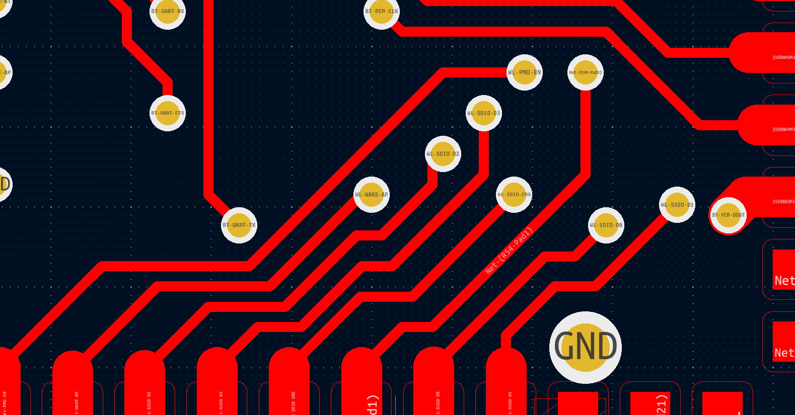
Figure 14 - Example of traces spaced too closed to each other for avoiding crosstalk
In this case, I recommend spacing them further apart to prevent the signal in one trace from coupling into another and generating noise.
If your board freezes or if an interrupt triggers unexpectedly, often referred to as “ghost signals,” this crosstalk can be a common cause. This is especially true when reset traces run close to fast signals, or when wake-up signals are placed near communication protocols.
Wherever possible, we should increase the distance between traces and utilize the board space efficiently to minimize electromagnetic interference. We will apply the same process across all the other layers as well.
Trace Branching - Stubs
Another important aspect we need to check is the creation of stubs or branches in the traces. This means we should ensure that each connection is made as a direct point-to-point connection, without splitting the signal trace into multiple parts.
For example, look at the traces shown here:
Figure 15 - Example of stub traces.
In this example, we have a signal that starts at one of the pins of the BGA (Ball Grid Array) and then splits into two branches through vias. One branch continues to connect to resistors on the right side, while the other branch goes through a via and a signal trace on layer 4.
The issue here is that when the signal reaches this split, its impedance changes suddenly. This change can lead to reflections, which are not good for signal integrity. These reflections can couple to other traces or structures on the board, potentially causing emissions.
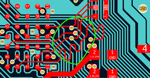
Figure 16 - Example of stub traces through via connection.
Additionally, depending on the signal's energy and harmonics, it may resonate along the trace segments, leading to more emissions. This can happen either directly or indirectly, as the resonating signals couple with other traces before radiating out.
To prevent these problems, we should avoid creating connections that split signals like this. If it’s unavoidable, we should ensure that any stubs we create are as short as possible. This minimizes the risk of resonance by making sure that only very high frequencies resonate, and these frequencies will have low energy.
Overall, this is another area that requires correction or improvement.
Time Matching vs. Length Matching
As we continue our analysis, let’s focus on an important aspect of signal integrity: length matching. Specifically, we'll discuss how it relates to crosstalk and ways to reduce energy dispersion, resonances, and crosstalk between traces.
One immediate observation is that the traces on this board are relatively close together, which poses a risk of unwanted coupling. To mitigate this, we should increase the spacing between the traces wherever possible.
Now, let’s touch on a crucial concept often overlooked by those new to high-speed routing: the difference between length matching and time matching. While length matching aims to ensure that traces are the same length, time matching is ultimately more important.
The key here is to ensure that signals arrive at their destination simultaneously, regardless of the physical length of the traces. The challenge is that signals routed on outer layers behave differently than those routed on inner layers.
For instance, the speed of a signal on an outer layer is generally faster because it propagates more in the air, whereas a signal on an inner layer travels through the dielectric material between layers. As a result, even if two traces are the same length, the time it takes for the signals to reach their destinations can differ significantly.
Focusing on time matching instead of merely length matching will help us ensure better signal integrity and reduce timing issues in our design.
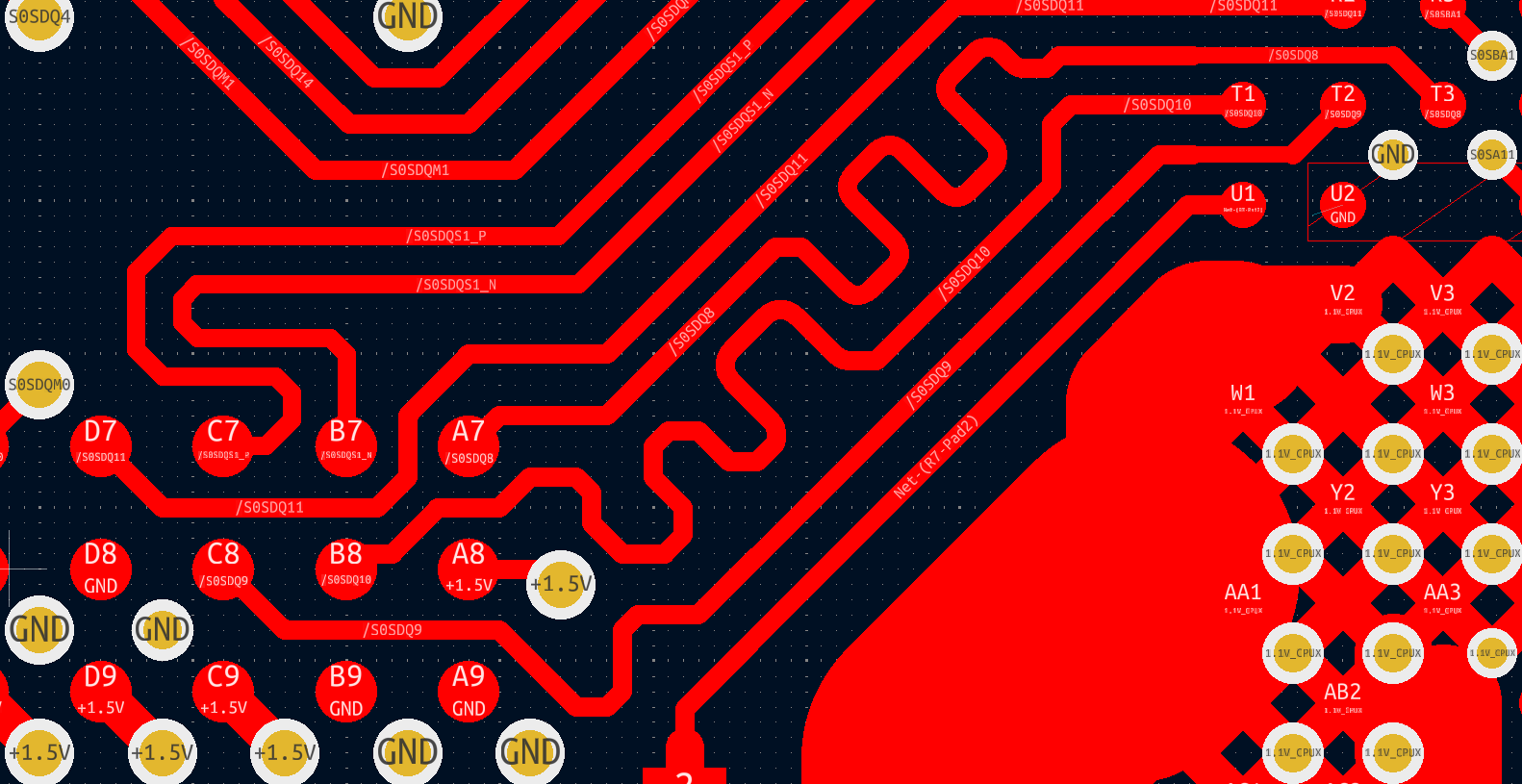
Figure 17 - Example of length matching traces.
When it comes to routing signals, there are important differences between using outer layers (microstrip) and inner layers (stripline). One significant aspect is how crosstalk behaves in these two configurations.
In microstrip routing, we need to consider both far-end crosstalk and near-end crosstalk. However, in stripline routing, we typically don’t experience the effects of far-end crosstalk. This difference is one reason why it’s often better to route high-speed signals on inner layers. Additionally, when signals are routed internally, the energy and emissions are better contained, reducing the potential for interference.
With this in mind, our main goal should be to focus on time matching instead of length matching. We also want to optimize the design of serpentine traces by making the "bumps" smaller and more frequent. By doing this, we increase the resonance frequency of the trace structure, shifting the problematic resonant frequencies higher and away from our signal bandwidth.
Moreover, smaller and more frequent bumps help reduce crosstalk between the legs of the serpentine. When the spacing between the bumps is shorter, there is less opportunity for the signal to couple with other traces, resulting in fewer fringe fields affecting the adjacent portions of the trace.
It’s essential to think in both the frequency domain and the time domain. Digital signals consist of multiple frequencies and harmonics, so we need to consider how they interact. A good rule of thumb is to space the bumps in the serpentine at least 3 to 4 times the trace width. The goal should be to have smaller and more frequent bumps rather than fewer, larger ones, as seen in this layout.
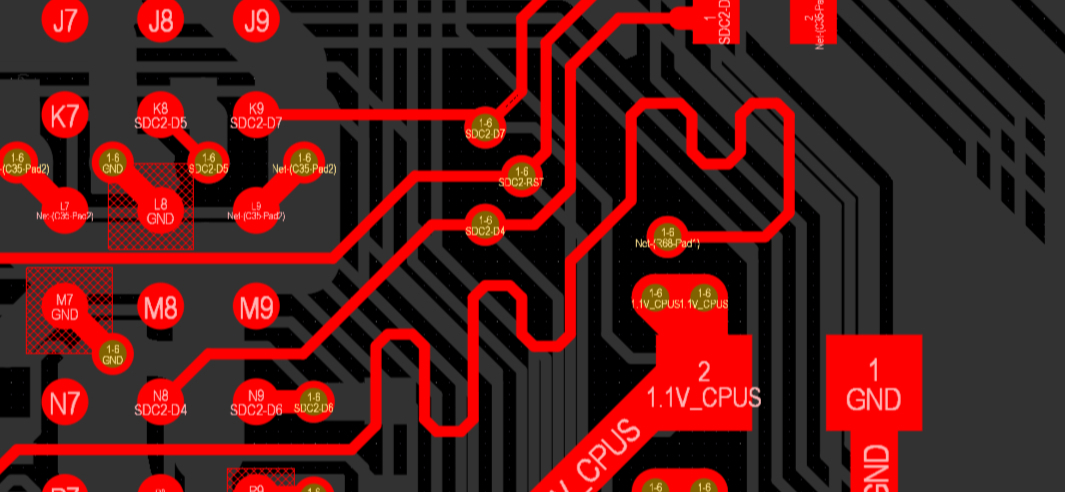
Figure 18 - Example of big "bumps" in length matching.
And then, of course, we have to simulate and actually calculate if we need more accurate values.
Controlled Impedance
The next point we want to cover, though briefly, is controlled impedance. I want to emphasize this because, when I was starting out, I didn't give it much importance, but it is one of the most critical aspects of PCB design.
Designing traces with controlled impedance means ensuring that the impedance between the signal trace and the return reference plane (RRP) remains constant throughout the entire length of the trace. This is typically achieved by maintaining a consistent width for the trace.
To calculate this impedance, you can use calculators that consider the entire geometry of the transmission line, including how the signal trace is positioned in relation to the RRP. I recommend consulting your PCB manufacturer for the correct values based on the specific board you plan to produce.
Once the manufacturer provides you with the necessary trace width to meet your impedance requirements, you should design the traces according to those specifications. For common signals, this is usually 50 ohms, but for specialized signals like high-speed protocols, it’s essential to check the specific requirements.
When we observe any change in the width of the signals, as shown in this case:
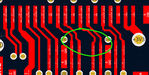
Figure 19 - Example of impedance mismatch along the traces.
We need to ensure that we use the same trace width throughout the design, and if we do need to change it, there should be a clear justification for that change.
If we don't maintain a consistent trace width, the signal may encounter reflections at the point of change, depending on the type of impedance mismatch we've created.
Impedance mismatches are critical to consider. Remember, impedance is simply the ratio of voltage to current. If we alter this ratio, we directly affect the signals being transmitted.
Power Section Analysis
The next aspect we need to analyze is the power section of the board. The main goal here is to ensure that the designer has used the space around the power converter efficiently to minimize current loops.
Figure 20 - Power Converter
One of the significant issues with power converters is that large current loops can behave like antenna structures, which can increase electromagnetic interference (EMI).
In the case of switching converters, their efficiency often relies on fast switching times. This rapid switching compresses the transition of energy from a high state to a low state (or vice versa) into a short time frame.
As a result, during this brief interval, we generate many more harmonics that contribute to these sharp signals. Instead of dealing with just one frequency component, we now have multiple frequency components. This increases the likelihood of any of these frequencies radiating based on the design of our structure.
It's essential to design our structure to contain these fields rather than allow them to escape. As discussed in the Radiated Emissions video, larger current loops lead to larger emissions. Thus, minimizing current loops is crucial.
A practical way to achieve this in a power converter, such as a switching DC/DC converter (and similarly for AC/DC converters), is to keep the input and output loops as small as possible. This typically means positioning the capacitors as close as possible to the pins, as well as the loops of the inductor and the diodes, depending on the topology.
In this design, we can see that the capacitors are all placed on the top layer. Before proposing any improvements, we should determine if the bottom layer can accommodate components in that area. If the bottom layer is usable, we might be able to position the capacitors closer to the pins. If not, we will need to explore options on the top layer.
The same principle applies to the processor. We must ensure that the decoupling capacitors are placed as close as possible to the pins they connect to. The goal is to reduce inductance as much as possible.
It’s vital to examine the current path, not just its proximity to the pin. Sometimes, moving capacitors to the other side of the board can reduce distance, but it may increase inductance due to the vias and traces. Therefore, we should optimize for low inductance, not just short distance.
I covered this topic in the Power Delivery Network (PDN) video, where I also discuss how to check the target impedance.
Layer 2 Analysis
For the top layer, we've already identified several areas for improvement, so let’s now examine the second layer.
Figure 21 - Layer 2
Overall, this layer appears to be in good shape. However, I would recommend increasing the space between the vias to allow for more copper to fill these areas.
If we don’t address this, we create gaps in the planes where no current can flow, leading to longer return current loops. This, in turn, directly impacts the emissions of the traces on the top layer. While we would need to simulate the exact impact, I believe it’s still worthwhile to make this improvement.
Aside from that, the plane is free from cuts, splits, or significant gaps under the traces on the top layer that could create impedance discontinuities. This is exactly the kind of structure we want.
I would also prefer to see an identical plane on layer 5, but as we observed, the designer has opted for a different approach.
Layer 3 Analysis
Now, let’s move on to layer 3.
This layer presents a mixed scenario. It features a large copper fill that covers the entire board, along with some high-speed traces. As I mentioned earlier, this space could be better utilized for signals. I would have relocated some of the signals from other layers to this layer.
Figure 22 - Layer 3
The recommendations I provided regarding serpentine routing and spacing between traces apply here as well. We can enhance the trace layout by removing the large copper fill, which would allow for more efficient use of the board space.
Another point of concern is the length of some of the traces. When designing traces, my goal is to keep them as short as possible to minimize current loops and reduce potential emissions issues at the frequencies of interest, which typically include those relevant to EMC tests and signal bandwidths.
Additionally, I would like to see more stitching vias connecting this copper fill to the reference return plane (RRP) on layer 2. This would create a more equipotential plane and raise the resonance frequency between these two planes. This is advantageous because we want to avoid resonances in cavities at lower frequencies, which could lead to EMI and signal integrity issues.
Placing more stitching vias—generally spaced 1/10 of the highest frequency component of the board—will be effective. While this is a general guideline, you’ll need to evaluate it based on the types of signals and rise times present, as well as the potential impact on manufacturing costs. A trade-off will often be necessary.
Nonetheless, increasing the number of stitching vias will help address the concerns mentioned.
Layer 4 Analysis
Now, things start to get a bit more complex in this layer. Here, we have a mix of digital signals, power traces, and copper fills.
The first step I recommend is to remove the copper fill to better understand how much routing space it occupies. Once we do this, we can see that there’s still room for improvements on this layer.
Figure 23 - Layer 4
One major issue is that the traces are routed too close to each other. We need to increase the spacing between them to reduce the risk of crosstalk and interference.
Another concern is that the power traces are running very close to the signal traces. This is problematic for a couple of reasons.
First, noise from the thick power traces can easily couple into the signal traces, leading to conducted and radiated emissions. Conversely, if the cables are not properly filtered, external interferences can impact the digital signals, causing immunity problems and affecting the board's performance.
To address this, I would increase the spacing between the power traces and the digital signals. We should also take advantage of the available board space to ensure that the fringe fields from the signals do not couple with each other.
The same principle applies to the power traces: we need to enhance the spacing between them to minimize coupling.
The recommendations I provided for the previous layers also apply here, so let’s keep those improvements in mind as we move forward.
Layer 5 Analysis
As I’ve mentioned several times, this layer, given the stack-up, should be dedicated exclusively to the Reference Plane (RRP). Therefore, it should ideally mirror Layer 2.
Figure 24 - Layer 5
We need to decide whether to add two more layers: one between Layer 4 and Layer 5, and another between Layer 5 and Layer 6, or if we should reroute the board differently.
Since there seems to be ample space on Layer 3, one option could be to route the digital signals from Layer 3 to Layer 4, then shift the current Layer 5 with the power traces to Layer 3. This would allow Layer 5 to serve as a full RRP.
If we can implement this change, we can avoid increasing the layer count, keeping costs down while still achieving effective results.
Additionally, the planes used on Layer 5 need to be justified. We must ensure that a plane is necessary instead of a power trace. This means checking whether the current and impedance requirements can only be met with planes. If not, we should replace the planes with thicker power traces, depending on the power requirements.
Another reason for replacing this layer with an RRP is that signals on Layer 6 and Layer 4 continuously cross the gaps between the planes. This situation leads to fields propagating through these gaps, and the return current loop becomes much larger.
As I explained in the Radiated Emissions video, larger loops lead to higher emissions from the board.
Therefore, we need to improve this aspect by ensuring we have a solid RRP without gaps, splits, or any other impedance discontinuities that could disrupt the integrity of the plane.
In summary, Layer 5 must be modified. We need to choose one of the solutions I’ve already outlined, whether it involves changing the stack-up or rerouting.
Layer 6 Analysis
Now, let’s examine the final layer: Layer 6.
To begin, I will remove the copper fill to better assess the usable space on this layer. Additionally, I will change the layer's color to improve visibility.
Figure 25 - Layer 6
As we can see, there is ample space available for routing. However, the issues observed in previous layers persist here as well.
The main concerns include:
- Traces Spaced Too Closely: The traces are too close to each other, which could lead to crosstalk and interference.
- Unnecessarily Long Traces: Some traces are longer than needed, which can increase inductance and reduce performance.
- Inefficient Use of Space: Overall, the routing space on the board could be utilized much more effectively.
One positive aspect of this layer is that there are fewer components located on this side of the board. This gives us more flexibility for routing compared to the top layer, where components occupy the majority of the space.
Conclusions
In this review, we've explored the fundamentals of conducting an EMI assessment for a Printed Circuit Board (PCB). While there's certainly more to the process, I aimed to provide a clear overview of what it involves and how quickly you can identify potential EMI issues simply by examining the layout.
💡 By the way, If you would like to master EMC/EMI design, we have a new training program here:
There, you’ll find details on how to apply for one of our exclusive programs designed to help you achieve that goal.