Return current doesn't follow the shortest path. It follows the path of least impedance — and as frequency rises, that path changes dramatically. Designing without accounting for this is designing with an invisible antenna on your board.


Every signal current that flows out of a source must return to that source. This is fundamental — not a guideline, Kirchhoff's current law. The question is never whether the return current flows, but where it flows. And the answer changes with frequency in a way that has direct consequences for every routing decision you make.
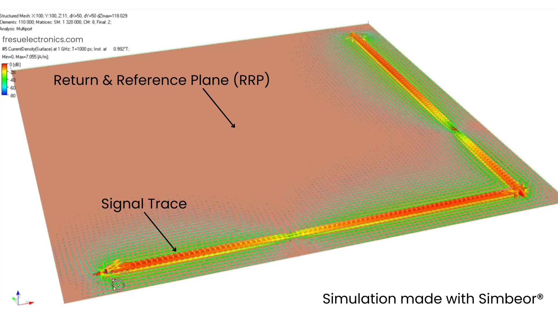
Figure 1 - Simulation of a two-layer PCB made with Simbeor®
Figure 2 - Example of a two-layer PCB stackup.
At low frequencies — below a few kilohertz — the dominant impedance in a conductor is its DC resistance. Return current distributes broadly across the available conducting area, taking the geometrically shortest path back to the source. The current loop is large, but at low frequencies, the radiation from a large loop is proportional to frequency squared, so the absolute radiation is still low.
This is why problems at low frequencies are rare — not because the current path is clean, but because even a large loop area radiates little at low frequencies.
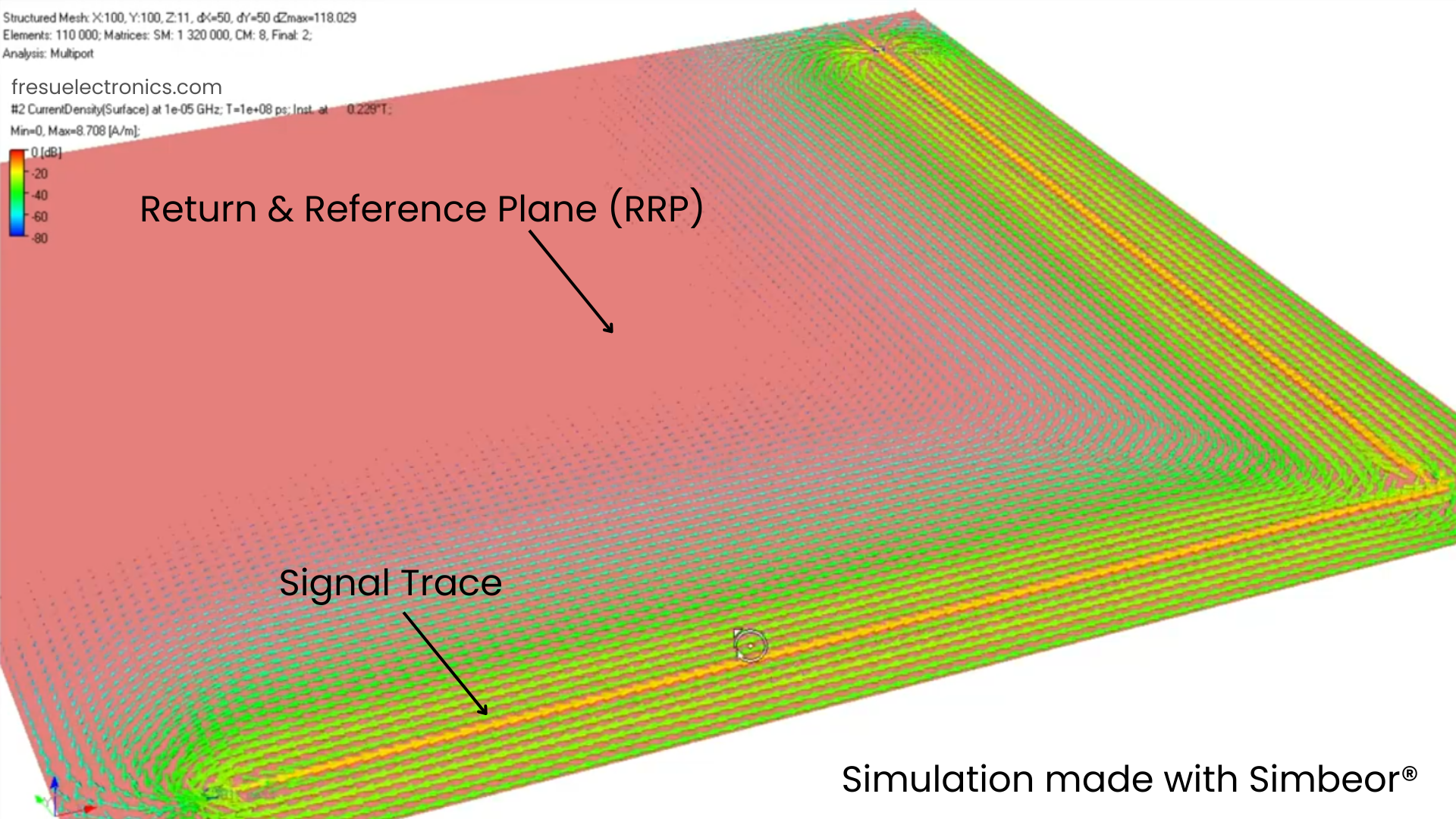
Figure 3 - PCB simulation with a 10kHz signal.
As frequency rises, inductive reactance (jωL) grows while resistance stays roughly constant. Above a few kilohertz, impedance is dominated by inductance, not resistance. Return current now seeks the path of least inductance — which is the path that minimises the loop area formed by the signal and its return.
In a PCB with a continuous reference plane directly beneath the signal trace, this means the return current concentrates in a narrow band directly under the trace. The loop area is minimised automatically by the physics. The field is contained. The board is quiet.
Figure 4 - PCB simulation with a 1 GHz signal.
At high frequency, the return current does not ask you where to go. It finds the path that minimises loop inductance — and if you haven't provided a clean one, it will find a dirty one.
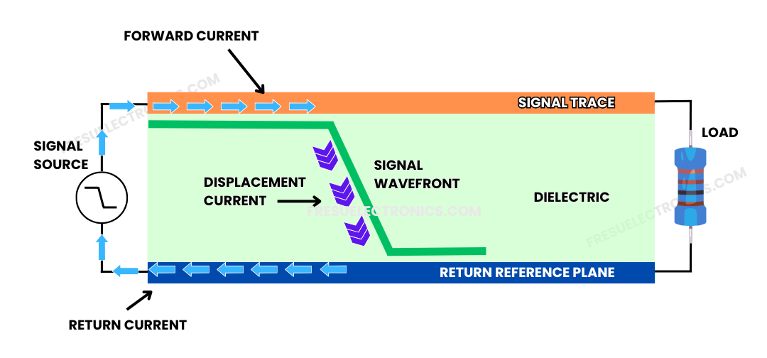
Diagram illustrating signal propagation and current flow in a transmission line, highlighting forward current in the signal trace, displacement current through the dielectric, and return current on the reference plane.
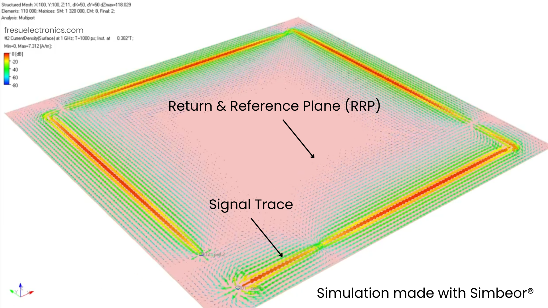
Figure 5 - PCB simulation with a 1 GHz signal and longer trace.
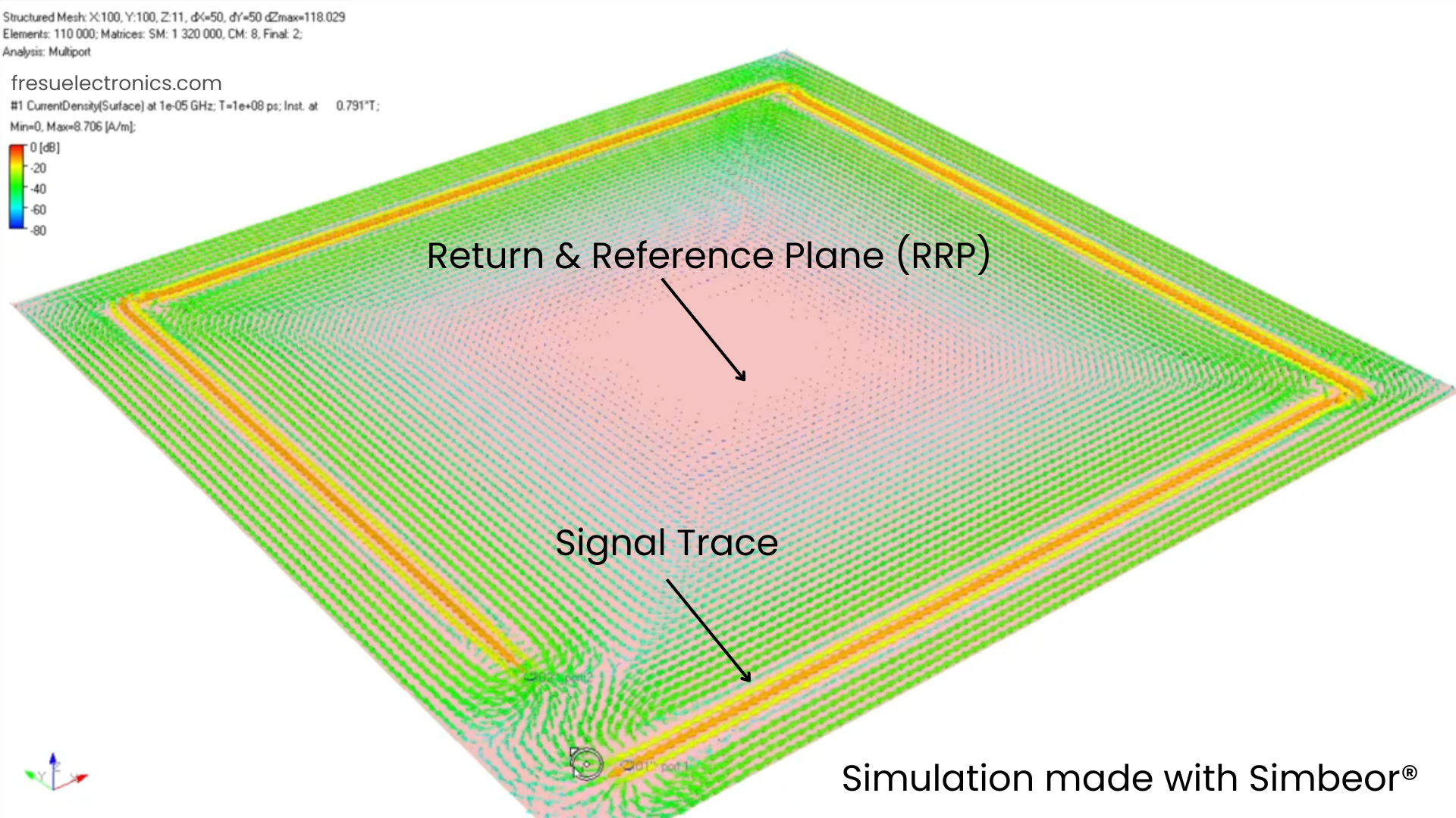
Figure 6 - PCB simulation with a 10 kHz signal and longer trace.
A slot, cut, or void in the reference plane beneath a high-speed signal trace forces the return current to detour around the interruption. The current cannot cross the gap capacitively at the frequency of interest — it must route around the edge of the slot. The resulting loop area is determined by the length of the slot, not the trace geometry. A 20mm slot beneath a 0.2mm trace produces a loop that is 100× larger than the trace geometry suggests.
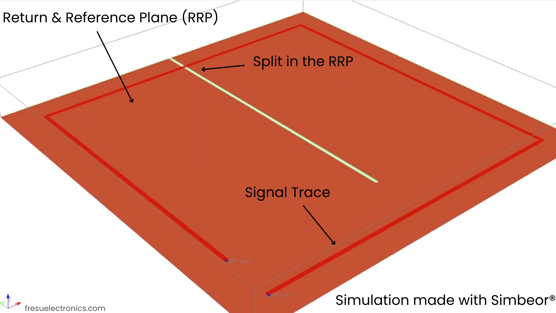
Figure 7 - PCB with a split in the Return and Reference Plane.
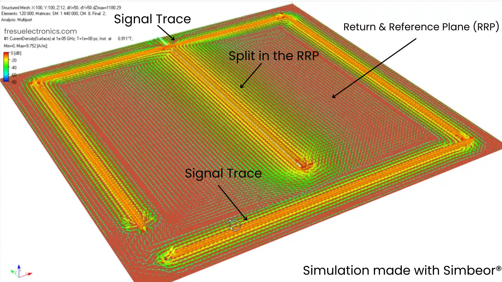
Figure 8 - Simulation of a 10 kHz signal routed across a split in the RRP.
This detour loop radiates in proportion to its area, the current it carries, and the frequency squared. A single slot in the wrong location can be the dominant emission source on an otherwise well-designed board.
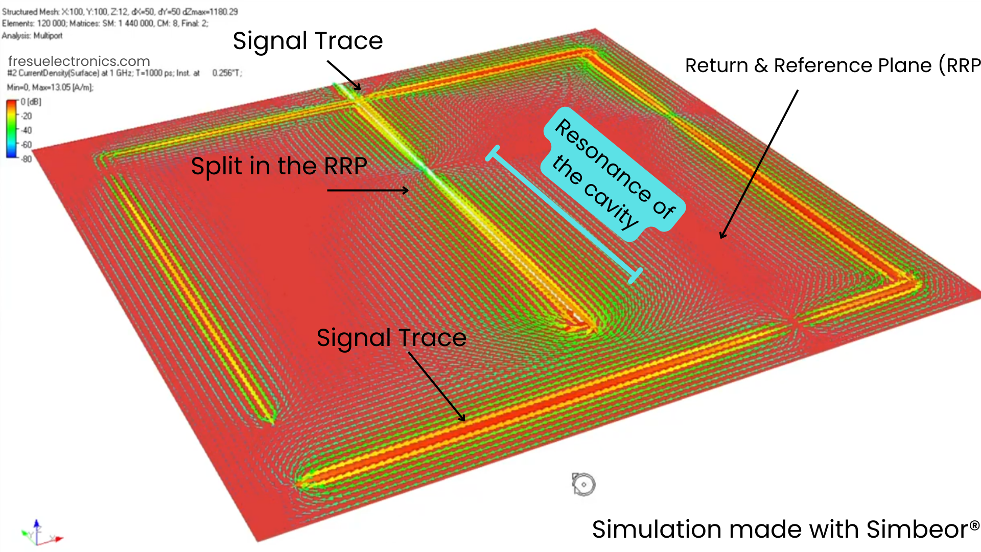
Figure 9 - Simulation of a 1 GHz signal routed across a split in the RRP.
Every time a signal changes layers through a via, its return current must also transition layers. Without a nearby return via, the current must travel across the plane surface to find the nearest stitching point — creating a loop. Place a return via within 1–2mm of every signal via for high-speed signals.
Never route a high-speed or high-frequency signal across a void, slot, or gap in the reference plane. This includes the gaps created by connector footprints, cutouts for mechanical components, and split plane boundaries. Reroute the signal or bridge the gap with stitching capacitors.
When signals must transition between layers, ensure the reference layer also transitions — either by remaining the same plane, or by providing a stitching capacitor between the two reference layers at the transition point. A signal that changes reference planes at a via effectively has no controlled return path at that via.
Before sending a board to fabrication, trace every high-speed and switching signal on the layout and identify the return path for each at the operating frequency. Where is the return current? Does it have a continuous, low-impedance path directly adjacent to the signal? If you cannot answer this for every critical signal, the board is not ready for fabrication.
Work directly with Dario to identify EMC risks at the design stage — before a €15,000–40,000 chamber session reveals issues that require a respin.
Get articles before they're published