The rule against 90-degree bends has been repeated so many times it has taken on the force of law. The justification usually given — that electrons accelerate at corners and cause radiation — is wrong. Here's what actually happens.


Few PCB design rules are as universally cited — and as poorly understood — as the prohibition on 90-degree bends. Ask any engineer why they should be avoided and you will likely hear: electrons accelerate at the sharp corner, causing electromagnetic radiation and reflections. This explanation is intuitive, memorable, and wrong.
Signals in a PCB trace at any modern operating frequency do not propagate as individual electrons making sharp turns. They propagate as electromagnetic waves guided by the conductor geometry. The actual concern at 90-degree bends is different, smaller, and frequency-dependent in ways the folklore doesn't capture.
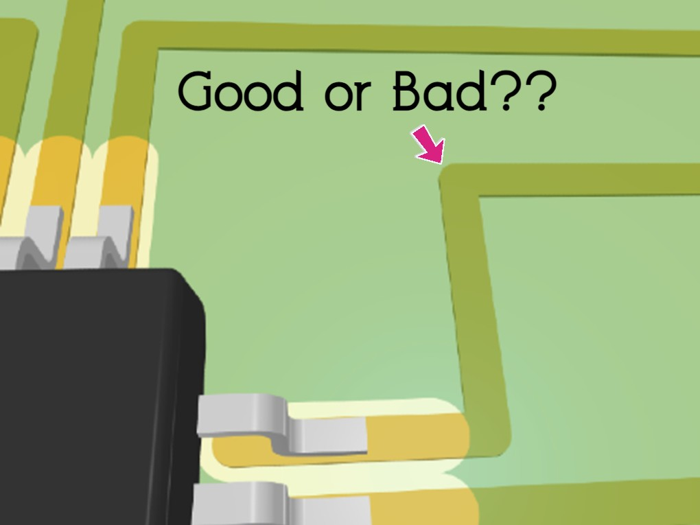
An electronic circuit board design is under scrutiny, with a highlighted corner and a caption asking if the 90-degree corner feature is good or bad.
A 90-degree bend in a trace creates a localised change in trace width. At the outer corner of a 90-degree bend, the effective width of the trace increases — the corner has more copper than a straight section of the same nominal width. This increased width corresponds to a small increase in capacitance per unit length, which produces a localised impedance discontinuity.
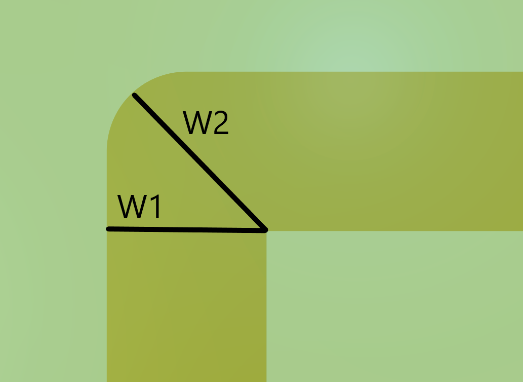
Diagram illustrating a copper trace rectangular corner, featuring two labeled lines, W1 and W2, that form a right-angled triangle highlighting the corner's geometry.
That's it. The concern is a small capacitive discontinuity — not electron acceleration, not radiation from the bend itself, not a fundamentally different electromagnetic phenomenon.
The corner doesn't radiate. The impedance discontinuity at the corner causes a small reflection. Whether that reflection matters depends entirely on your signal frequency and trace length.
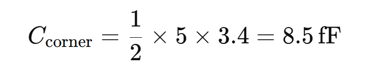
A reflection caused by an impedance discontinuity becomes significant when the electrical length of the discontinuity approaches a meaningful fraction of the signal wavelength — typically when the discontinuity length exceeds λ/20. For a 90-degree bend on a standard PCB trace, the excess copper at the corner is on the order of 0.5–1mm. At what frequency does 1mm become λ/20?
At 15 GHz. For the vast majority of digital and mixed-signal designs operating below 5 GHz, the 90-degree bend is electrically invisible. Its capacitive discontinuity is too small relative to the signal wavelength to cause measurable reflections or signal degradation.
If 90-degree bends are not the primary source of signal integrity problems, what is? The answer is trace geometry changes that create meaningful impedance discontinuities: changes in trace width without a corresponding adjustment in reference plane distance, vias (which introduce significant inductive discontinuities), stubs on unused via barrels, connector footprint geometries, and — most importantly — return path discontinuities caused by splits or voids in the reference plane beneath the trace.
A trace routed across a slot in the ground plane will have far worse EMC performance than a trace with a hundred 90-degree bends over a continuous, uninterrupted reference plane.

Close-up view of a circuit board, showcasing intricate components and pathways, illuminated by soft, ambient lighting.
For designs operating above 10 GHz — millimetre-wave, high-speed serial links above 25 Gbps — the capacitive discontinuity of 90-degree bends does become relevant and mitigating it with chamfered or curved bends is justified. For most practical designs operating below this threshold, the choice between 45 and 90 degrees is an aesthetic preference, not a functional requirement. Spend the routing effort on return path continuity, via placement, and reference plane integrity — these have measurable impact at the frequencies you are designing for.
Work directly with Dario to identify EMC risks at the design stage — before a €15,000–40,000 chamber session reveals issues that require a respin.
Get articles before they're published