

Action list:
1. Get the New EMI Quick Fixes Guide - 2025
In this lesson we dive deep into the review of the iMX8 processor PCB, focusing on Electromagnetic Compatibility (EMC) and signal integrity.
We start by analyzing the stack-up of the board, identifying potential issues with mixed signal layers, power planes, and return reference planes. Throughout the lesson, we will highlight specific problem areas, and provides recommendations to enhance board design for better EMC compliance and signal integrity.
Stackup analysis
The first aspect to examine is the board's stack-up. Understanding the stack-up is essential to evaluate how the fields will behave in this system on module. Analyzing the stack-up reveals several key details, starting with the fact that it consists of the following layers:
- Layer 1 - Mixed Signals
- Layer 2 - Power Plane
- Layer 3 - Power Plane
- Layer 4 - Signals
- Layer 5 - Signals
- Layer 6 - Mixed Signals
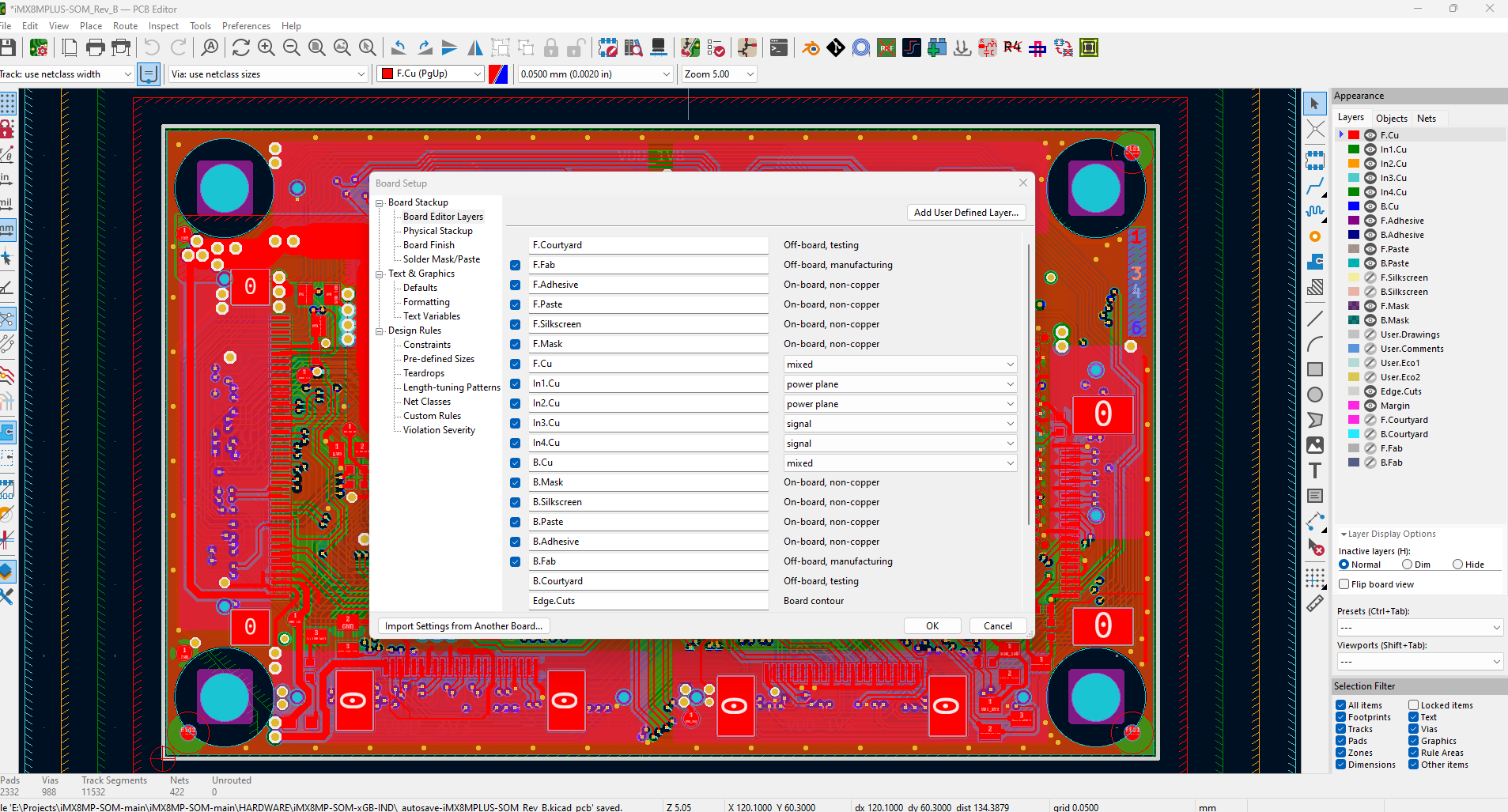
Figure 1 - Stackup of the board.
At first glance, there could be potential issues. A mixed signal layer means that both signals and power are integrated on the same layer. Directly beneath it is a power plane, which ideally should be a return reference plane (RRP). However, what catches the attention is the additional plane on layer three. This plane could potentially be another power plane, but there’s uncertainty around its exact role.
🔓 Ideally, we want to ensure that each signal and power layers are paired with their respective return reference plane (RRP).
This principle is crucial for maintaining signal integrity and preventing electromagnetic interference (EMI). Replacing a return reference plane with another signal layer to reduce costs might seem appealing, but this approach often backfires. While it may appear to save money by eliminating a layer, the actual costs become evident during EMC tests or signal integrity checks.
🔓 It is important to remember that a signal voltage is defined by two potentials: the signal's active potential and its reference potential.
If one of these potentials is removed, we’re left with only one potential, which means there’s no longer a voltage difference to define the signal.
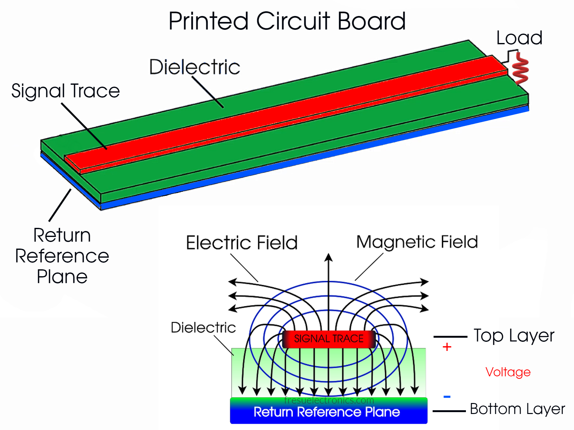
Figure 2- Electromagnetic Fields in a two-layer PCB.
Without both potentials, a usable signal may not exist, or any signal present will likely rely on parasitic elements. These parasitics can provide a return path to close the current loop, but this compromises signal quality. When selecting a stack-up, it is essential to think in terms of pairs.
🔓 Signal (and power) layers should always be paired with their corresponding return reference planes.
This pairing forms the foundation of effective stack-up design and helps prevent issues with signal integrity and electromagnetic compatibility.
Digital signal layers should always be placed adjacent to a return or reference plane. Without a reference plane, a single signal layer effectively functions like an RF board, promoting signal emission rather than supporting digital or mixed-signal designs. This approach can lead to significant electromagnetic compatibility issues and should be avoided. When a return reference plane is absent next to the signal, significant radiation can be emitted. This concept is explained in greater detail in the 'Radiated Emissions' lesson available in the courses and blog.
From a manufacturing perspective, the stack-up should be designed as a mirror image, with one side of the board reflecting the other. For a six-layer board, as in this case, if a return reference plane is placed on the second layer, another return reference plane should be placed on the fifth layer. This principle of symmetry applies to other layers as well. Such symmetry is essential to ensure consistent and predictable electrical and mechanical behavior of the board.
A symmetrical stack-up is particularly important for the board's thermal behavior. An asymmetrical stack-up can cause uneven heating, leading to warping. This warping may place stress on solder joints, potentially causing components to detach from the board. Such mechanical failures could be easily avoided with a well-designed stack-up.
To prevent these issues, it is essential to aim for a symmetrical stack-up. Pair each signal layer with a return reference plane and strive to make the overall stack-up as balanced as possible. A symmetrical design enhances not only electrical performance but also the mechanical integrity of the board, ensuring greater reliability and robustness over time.
Proceeding with the analysis, the layers and their arrangement should now be examined more closely to better understand the setup. The first pair of layers consists of the first signal layer and the second layer, which serves as the reference plane for the first layer. The third layer, at first glance from the sstakcup manager, appears to be a power plane. However, upon closer inspection, it seems to function more as a signal layer with some copper pours integrated into it.
Figure 3 - Layer 3 of the PCB.
This third layer is positioned at the same distance from the second signal layer as the first signal layer. With this type of stack-up, it becomes clear that the third layer, which acts as a signal layer, should be paired with a return reference plane, which will help ensure proper signal return current and voltage reference.
In this case, maintaining an appropriate distance between layers is even more important. The signal on the third layer must not interfere with the signal on the fourth layer. If the distance is too small, there is a risk that signals on one layer will start interfering with signals on other layers, leading to unwanted coupling and noise. Therefore, it is recommended to reduce the distance between the second and third signal layers to create strong coupling between the signal and its return reference plane.
By optimizing this distance, we can achieve a situation where the return current, and the voltage reference for each signal is confined to its designated area, reducing the potential for crosstalk with signals on layer four.
The use of the second layer as a return and reference plane for both the first signal layer and the third layer, is made possible by the skin effect, which ensures that the return current will flow along the portion of the plane directly beneath each signal. For example, the signal on the first layer will create a return current in a localized region of the return reference plane on the second layer, and the same will happen for the third signal layer.
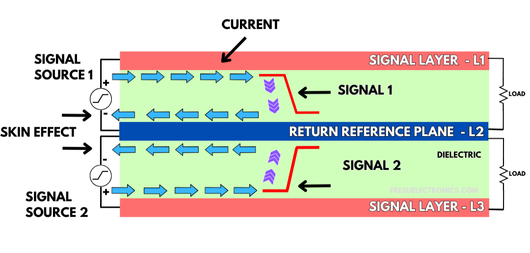
Figure 4 - Example of skin effect when a return reference layer is used in a PCB stackup.
To further reduce the risk of interference between signals, if needed, we can also adjust the stackup to ensure that the spacing between the signal layer and the return reference plane, ensuring optimal coupling. The goal is to reduce the distance as much as possible without causing unwanted interference between adjacent signals.
Moving to the next layer, layer four, it is similar to layer three in that it is also composed of digital signals, but it also features some planes, likely power or ground planes. Since layer four also carries digital signals, the next step is to place another return reference plane on layer five, similar to the one on layer two. This will help ensure proper coupling for the signals on layer four.
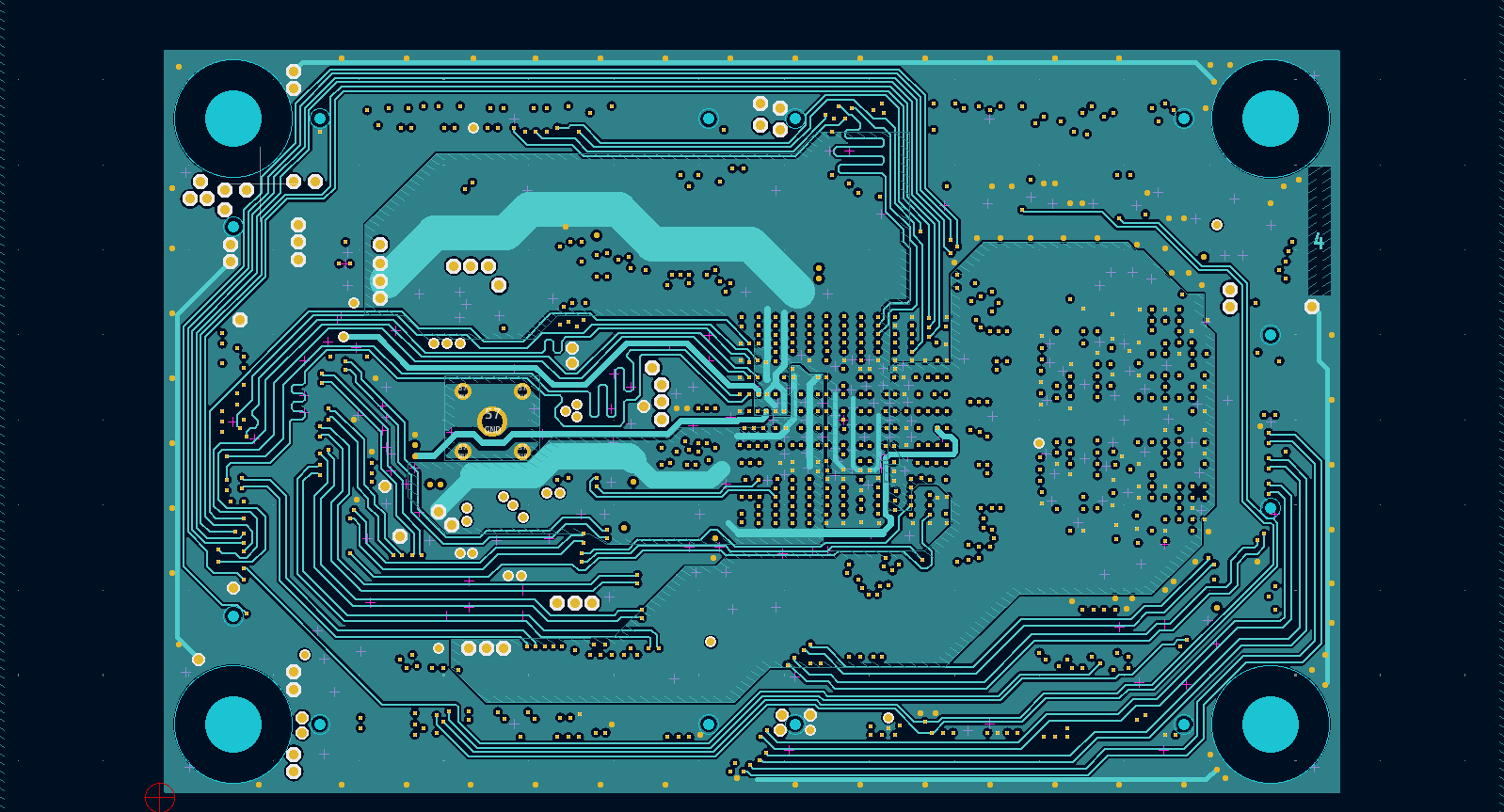
Figure 5 - Layer 4 of the PCB.
Upon closer inspection of layer five, we see that while it contains some planes, they may not be sufficient to effectively serve as the return reference plane for the signals on the layer four and on layer six. In fact, there are some potential issues with the planes here that could cause problems, and these will become clearer once we analyze the setup in more detail.
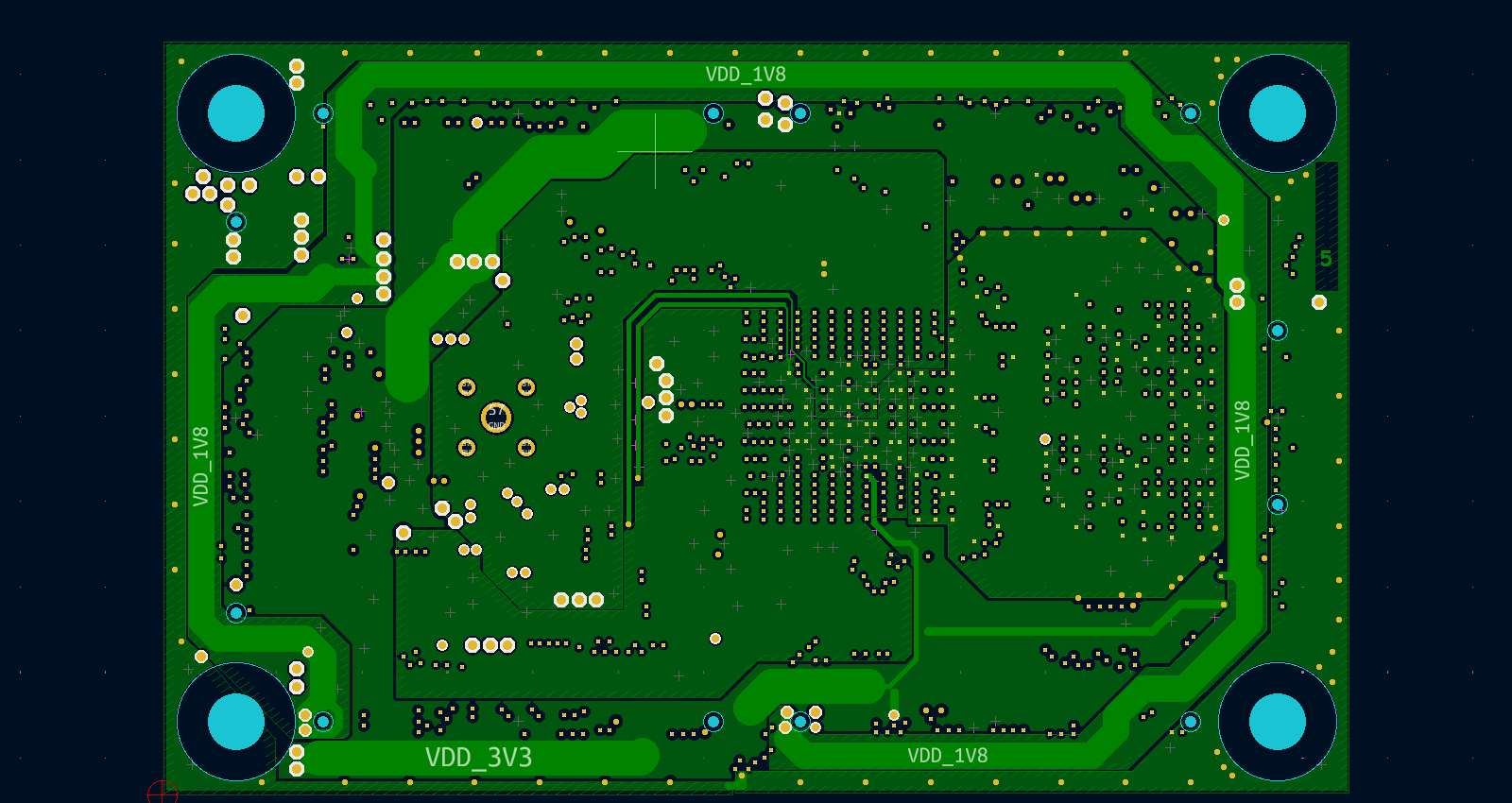
Figure 6 - Layer 5 of the PCB.
The primary concern arises with the signal layers on layers four and six, which rely on a stable return reference plane for proper operation. However, the planes on layer five may not provide the optimal reference for these layers, and this mismatch could lead to EMI and signal integrity issues.
Figure 7 - Layer 6 of the PCB.
Now that we have an overview of the stack-up and its associated potential issues, we can proceed to analyze each layer in greater detail. By breaking down the design, layer by layer, we can better understand the specific challenges and opportunities for improvement within the board.
💡 By the way, If you would like to master EMC/EMI design, we have a new training program here:
There, you’ll find details on how to apply for one of our exclusive programs designed to help you achieve that goal.
Layer 1
Let's start by examining the top layer more closely. The first issue that stands out is the presence of copper pours, which can potentially lead to problems. In this design, the goal seems to be to use stitching vias to connect the planes, especially the return and reference plane (RRP) located on the second layer.
Figure 8 - Layer 1 of the PCB.
While this is a common technique, it does introduce some risks, especially regarding the formation of certain geometries that may create unintended antenna patterns. For example, consider the section shown in Figure #. The design includes only a single stitching via, and a segment of the copper pour is present that can act as an antenna.
Another area where a similar issue arises is where a part of the copper pour, with just one stitching via, extends out and forms a potential antenna pattern. This type of geometry is concerning, as it can lead to performance issues, particularly in high-frequency designs, where antenna-like behavior can cause significant problems.
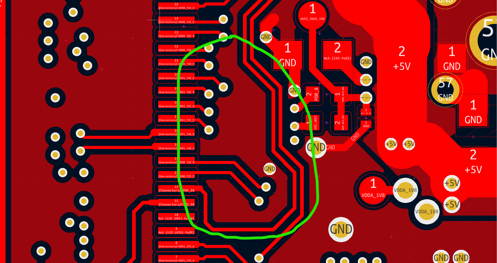
Figure 9 - Example of antenna-like structure.
Another problem here is related to manufacturing. Some of these copper features are quite thin, which raises the possibility that they might not be manufactured correctly. This thinness could lead to reliability issues or, worse, cause the design to fail during production. Beyond the manufacturing concerns, the main issue lies in how these geometries can behave electrically. With just a single stitching via, there is no effective path for the return current to flow properly. This can result in these sections of the copper pour acting like an antenna, which is problematic.
🔓 Without a complete return path, the geometry becomes a potential source of noise and interference.
The recommendation here is to remove these problematic sections from the design. For instance, the portion highlighted in Figure #, with only one stitching via, should definitely be reworked. These geometries can create voltage drops between the points where they are connected to the return reference plane and where they extend out. This difference in impedance between the two points can lead to significant issues and the creation of common-mode voltage sources.
The voltage drop that occurs due to the impedance mismatch introduces noise into the system. This noise then couples to the return reference plane, creating common mode currents that can affect the performance of the circuit and the failure of EMC tests.
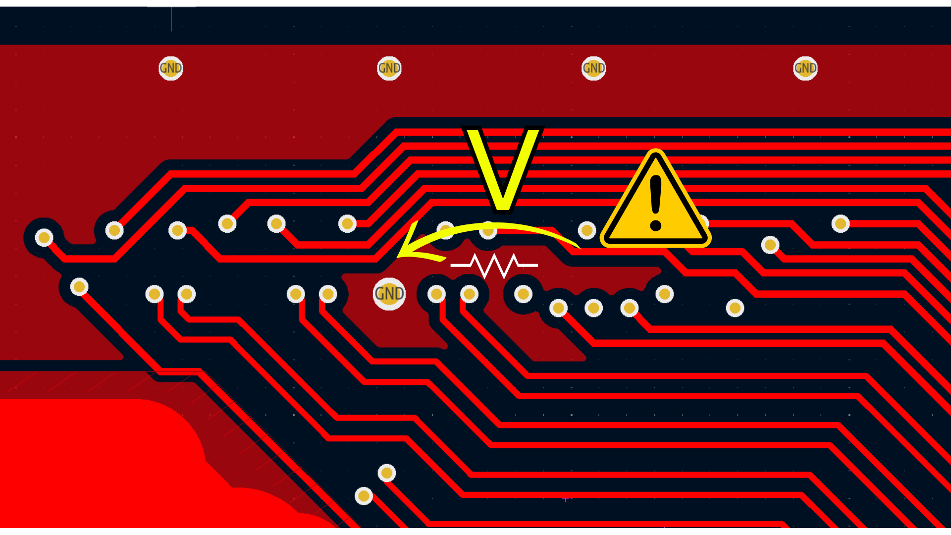
Figure 10 - Another example of antenna-like structure.
Furthermore, when a cable is connected to the return and reference plane, and when noise couples to it, this cable can act as an extension of the board itself, effectively turning it into an antenna. This leads to radiated emissions that can interfere with other nearby electronic devices, which is something we definitely want to avoid.
The presence of such antenna-like patterns in the design can also increase the risk of electromagnetic interference (EMI), especially as frequencies rise. Therefore, it is essential to eliminate these types of features at all costs. In this case where copper pours are used, the intention seems to be to maintain copper balance across the board.
However, given the high density of traces in this area, the board is unlikely to experience warpage or similar mechanical problems, and copper balance is not likely to pose a significant issue in this design. The greater threat in this design is posed by the antenna patterns, which represent a clear risk to the design’s performance and should be addressed immediately to ensure the system functions as intended.
Another aspect that should get our attention is the variation in trace width on one of the signal traces. On one side of the trace, we have a width of 0.08 millimeters, while on the other side, the width increases to 0.1 millimeters. Ideally, it’s important to maintain a consistent impedance throughout the traces. This consistency helps ensure that when the signal is propagating along the trace, it doesn’t encounter any impedance changes that could lead to problems.
Figure 11 - Example of impedance mismatch.
When the signal reaches a point where the impedance changes, such as from 0.08 millimeters to 0.1 millimeters, it will experience an impedance mismatch. This causes part of the signal to reflect back, leading to a reflection at this point. These impedance discontinuities, depending on the signal under analysis, are problematic because they disrupt its smooth propagation, causing noise and distortion.
🔓 When designing traces, we want to maintain controlled impedance, meaning the impedance should be constant across the entire length of the trace!
The trace can be thought of as a transmission line for the signal, with the impedance representing the characteristic impedance of that line. For the signal to propagate properly, the impedance from the beginning to the end of the trace, as well as at the load, must remain consistent. If the impedance changes along the trace, the signal may experience reflections, particularly when it encounters a segment with a different impedance.
For example, if the impedance is 50 ohms at one point along the trace but changes to 30 ohms at another, we create a mismatch between the points, which can potentially results in a reflection. If the instantaneous impedance changes at any point along the trace, the characteristic impedance is no longer consistent, and the transmission line loses its defined impedance.
To avoid such issues, it is essential to minimize changes in impedance wherever possible. While some minor reflection may occur due to impedance mismatch, especially depending on the signal type, significant changes in impedance should be avoided.
A positive feature of this design, is the relatively large distance between the differential pairs traces. This spacing is beneficial because it reduces the risk of crosstalk, which can occur when signals from adjacent traces interfere with each other.
Figure 12 - Another example of antenna-like structure surrounded by high-speed signals.
However, there are still some areas of concern. For instance, in certain places, the spacing between signal traces is quite dense. While this may still be acceptable, it’s something that needs to be tested and verified, as the density could lead to issues such as crosstalk. In this section (see Figure #), the distance between the traces is about the width of a single trace, which is definitely too small. This reduced spacing could result in signal integrity issues, and in this case, it would be definitely recommended to adjust the layout to increase the distance between these traces to at least two to three times the trace-width.
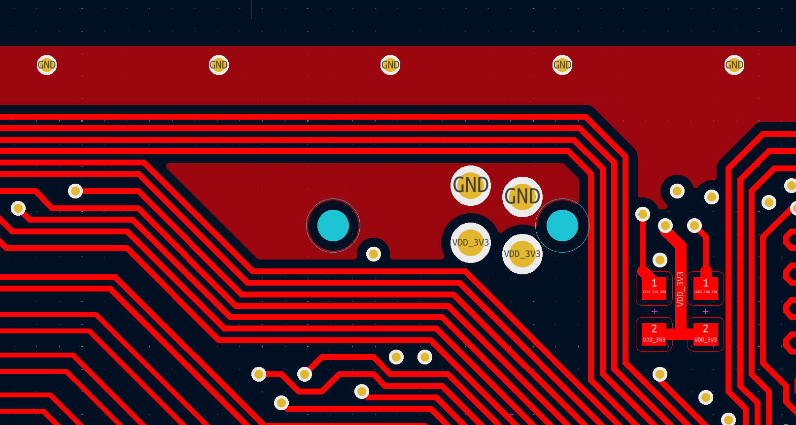
Figure 13 - Example of traces routed too close together, promoting signal crosstalk.
Moving on to the next issue, even though stitching vias are being used in this design, it is recommended to eliminate the sections of the copper pours and increase the distance between the signal traces, particularly in areas where the traces are not routed as differential pairs.
For instance, in Figure # we have a clock signal, which is particularly susceptible to coupling with adjacent traces. This can easily lead to crosstalk between the signals, which is undesirable. Therefore, it would be beneficial to increase the spacing between these signal traces to reduce the likelihood of interference. This is because clock signals are typically trapezoidal, requiring a high harmonic content to construct the waveform. Consequently, a higher amount of energy is transferred in a short period of time.
To minimize this crosstalk effect, we want to maximize the distance between these traces. Increasing the distance between the traces that carry sensitive signals, like clock signals, helps prevent interference and ensures better performance.
Another common issue, which might seem more advanced but is actually a fundamental practice, is the lack of return reference vias (RRV). Return reference vias are those connected to the return reference plane (RRP). These vias are important because, when the signal transitions from one layer to another, such as from the top layer to the bottom layer, it needs to maintain a stable reference potential and provide a lowest impedance path for the return current.
🔓 Return and reference vias (RRV) provide the path for the return current and the reference potential when the signal transition from horizontal propagation to vertical propagation.
The problem here is that when the signal transitions from one layer to another, it can lose its reference if there is no return path established. The return current, which is crucial for the signal's propagation, needs to follow a path that maintains the reference voltage. The signal needs a clear path to follow, that ensures the voltage between the return reference plane, and the signal trace is consistent.
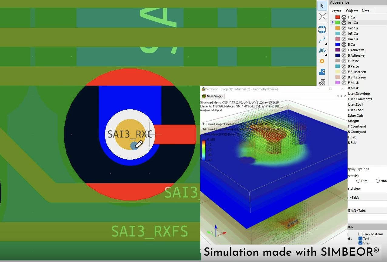
Figure 14 - Example of signal vias without a return and reference via adjacent to it.
Unfortunately, in this design, we see that many of the signals lack return reference vias. When signals cross the stack-up without these vias, they can lead to radiation emissions, which can spread throughout the planes and their cavities, and cause resonances. This could result in unwanted radiated emissions from the board that interfere with other parts of the system, or signal integrity issues that interfere with the internal operation of the device.
The lack of return reference vias when transitioning between layers is a significant issue. These omissions can lead to higher levels of radiation and noise, which can degrade the overall performance of the design. While the rest of the design seems to be in good shape, addressing this issue of transitioning without return reference vias is crucial for ensuring the system functions correctly without emitting unwanted interference.
Layer 2
Moving to layer two. As we mentioned before, this layer was almost in good shape, but there are still some issues to address. The problem here is that the plane is not a full solid plane but it presents a split between two planes.
We have one plane here, which is connected to the GND net, used as return and reference, but there’s also another plane here that’s still connected to the GND net. However, between these two planes, there’s a noticeable gap.
Figure 15 - Layer 2 of the PCB with the split of the planes highlighted.
This gap between the two planes is an issue because we have signals running on the top layer that cross over this split. When the signal reaches this split, it essentially loses its reference potential underneath, and it no longer has a path for the return current to follow as it crosses this point. The fields associated with the signal will start to spread throughout the gap. This gap between the two planes creates what we call a cavity. The cavity is the void between the planes, and this is where the signal can start to behave unpredictably.
When the signal crosses this gap, the fields that were initially confined to the plane, start to spread out into this cavity. The return current also loses its reference, causing it to find an alternative path to complete the loop. The spreading fields in the cavity can cause signal integrity and EMI problems, as they can couple with the surrounding signals on the board. This type of coupling can lead to crosstalk, where signals interfere with each other, causing noise and distortion.
Another problem arises because the cavity between the planes, depending on the signals, behaves like a resonant cavity. As the fields are injected into this cavity, they can cause the cavity to resonate at a certain frequency. This can create issues in terms of electromagnetic compatibility (EMC) because the cavity acts as an antenna and can radiate unwanted emissions. These emissions can be detected when measuring for EMC compliance, which could lead to further complications down the line.
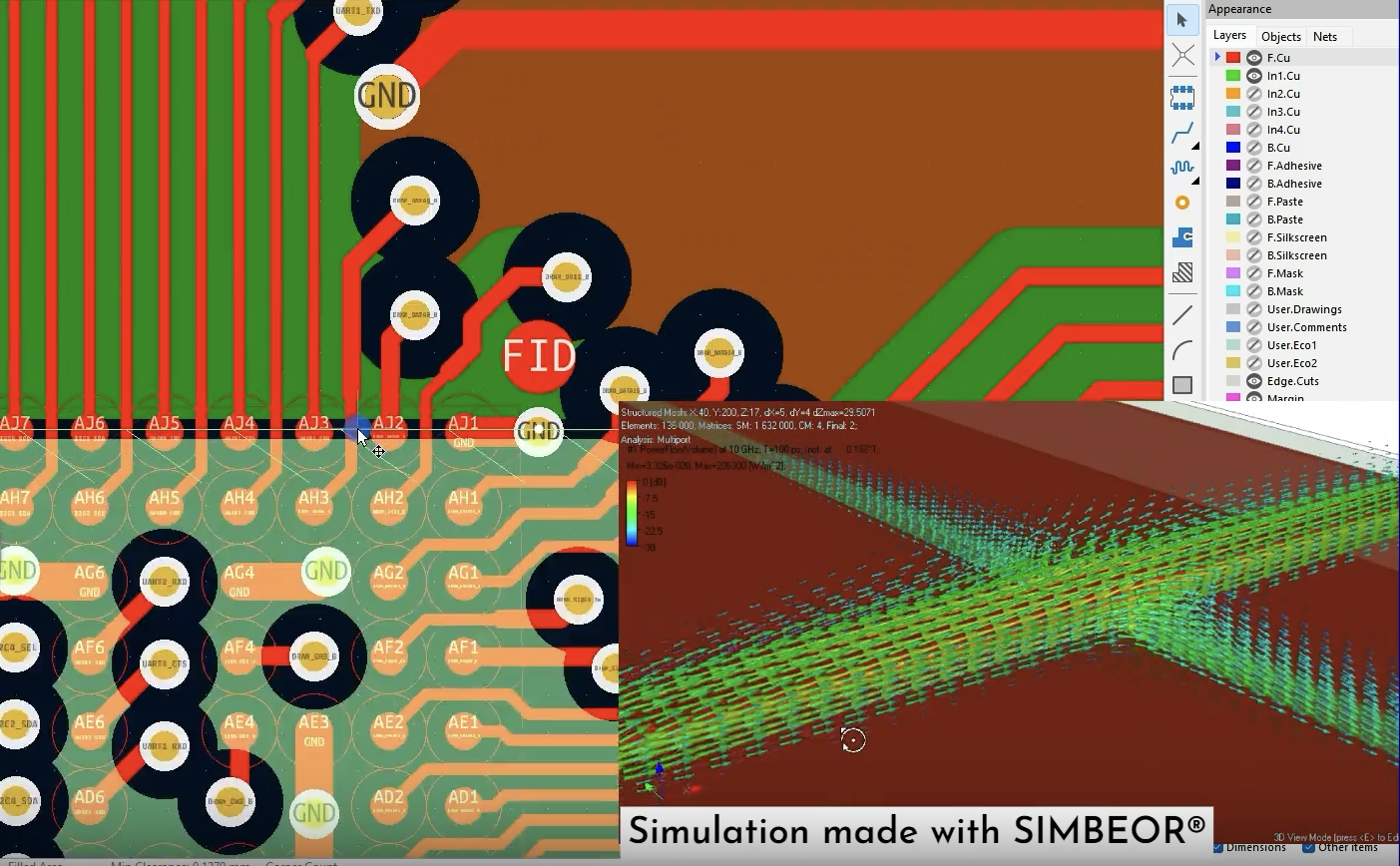
Figure 16 - Signals crossing the split in the plane, and simulation of the behaviour on the right corner.
This resonant cavity is problematic because it can generate a frequency that radiates outside the board. The impact of this issue depends on the design and how the cavity responds to the trapped energy. While it may not always be easy to measure or predict, it remains a concern that must be addressed. The fact that signals pass through the splits in the planes makes this a high-risk area. Without a proper return current path and attention to the cavity between the planes, the design could face issues with signal integrity, crosstalk, and even EMC compliance.
🔓 Allowing signal traces to pass through splits between planes is not good design practice.
To fix this, the design would need to be modified to eliminate the split, and ensure a proper return current path at all times.
Looking at layer two, there's another issue with large gaps between the vias, which could easily be avoided. The solution is simple: increase the distance between the vias. By spacing them further apart, the copper field can fill the area between them, ensuring the current flows properly. When the gap is too large, it creates a void where the current can't flow. This forces the current to take another path, which can cause problems like bigger current loops.
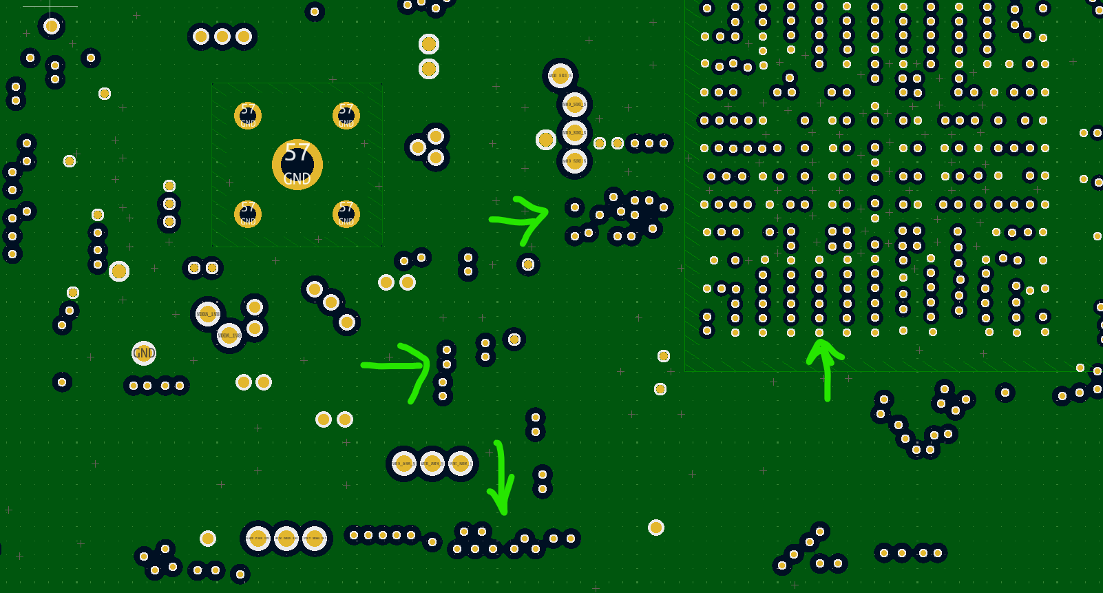
Figure 17 - Example of vias placed too close to each other, limiting the current flow.
Increasing the distance between the vias helps the return current flow more smoothly. This adjustment ensures the current has a clear path without "jumping" gaps. This approach should be applied to similar spots on the board to prevent the issue from occurring elsewhere. Such a small change can greatly enhance the design and performance of the system.
Another good feature of this design is the use of stitching vias along the edge of the board. This creates a Faraday cage around the entire perimeter, with the stitching vias acting as a barrier to protect the board from external electromagnetic interference (EMI). This approach is helpful in reducing radiated emissions and improving the board's overall shielding.
However, there's an important issue to consider:
Where are the stitching vias connected?
The effectiveness of shielding depends on how the vias are connected across the board layers. If stitching vias are only connected to one layer, they can cause problems. When connected to just one plane, especially with high-frequency signals, the vias can act like antennas. They may resonate at certain frequencies, leading to EMI or interference instead of improving shielding. To avoid this, it's important to connect the vias properly across all relevant layers of the board.
Layer 3
Looking at layer three, the first thing to do is remove these polygon pours. They take up valuable space that could be better used for signal routing. The layout is quite dense, with little space between traces, which can lead to potential issues, especially crosstalk.
Figure 18 - Layer 3 of the PCB.
When traces are placed too close together, their electric fields can couple, causing noise to affect nearby nets and potentially leading to signal integrity issues. If these signals are connected to cables, the coupling could also cause EMC problems. To avoid this, it's recommended to remove the "GND" polygon pours, and use the space more effectively to increase the distance between traces, minimizing the chance of unwanted coupling.
Especially with fast-switching signals, it's important to focus on trace spacing. Fast signals are more likely to cause noise and interference, so extra care is needed in the layout design. Ensuring enough space between traces helps minimize cross-coupling and interference.
Additionally, stitching vias have been used in some areas to connect the polygon pours and prevent them from acting like antennas. This is a good practice, but it’s important to consider how the vias are used. While some stitching vias are fine, others may not be ideally placed or may not provide the necessary return paths for the current. These should be reviewed carefully to ensure they don’t cause further issues in the layout.
Layer 4
Moving on to layer four, the design can be improved by removing some copper pours and using the space more effectively. One issue is that power is supplied to the DRAM through this layer, as shown by the VCC DRAM connection. However, the return and reference plane is on layer two, which is less than ideal because the power plane on layer four isn't directly next to a return reference plane.
Figure 19 - Layer 4 of the PCB.
In a properly designed layout, the power and ground planes should be next to each other for proper energy delivery. However, in this case, the power plane is on layer four, and the ground plane is two layers away on layer two. This creates a problem, as the forward current and return current must travel a greater distance, enlarging the current loop, and having the displacement current crossing two dielectric layers before reaching the return and reference plane. This separation weakens the return current path and can cause issues with signal integrity and electromagnetic compatibility (EMC).
To better understand the issue, it's important to know that electric fields are created between the power plane and the return reference plane, not in the copper itself. When the return and reference plane is far from the power plane, it becomes harder for the current to flow effectively, leading to poor energy delivery to the DRAM. This setup is likely to cause EMC problems because the electric and magnetic fields behave poorly in this configuration. Electromagnetic compatibility depends on how these fields interact, and this stack-up makes it harder to control them.
🔓 When choosing a stack-up, it's important to keep signal and return reference planes close together, and similarly, power and return reference planes should always be adjacent.
This ensures a clear, low impedance path for the current to return to the source. While cost considerations may lead to reducing the number of layers, choosing a stack-up like this could result in higher costs later to resolve EMC issues. For example, expensive EMC testing may be needed, and if the board fails, a costly redesign may be required to meet the necessary standards.
This board is sold as an industrial module, and the layout may have been chosen due to budget constraints, with limited focus on electromagnetic compatibility. The stack-up choice could be a key reason it struggles to meet EMC requirements for both industrial and domestic standards.
Layer 5
Moving to layer 5, the power plane should be a full return reference plane instead, with no splits or cuts. Currently, the power plane is fragmented with unnecessary splits, which complicates the current path. The return current has to travel through large sections of these broken-up planes, and as signals cross the splits, they will experience increased radiation, both differential and common mode. The return current will struggle to find a clean path to the ground plane, leading to inefficiencies and signal integrity issues.
Figure 20 - Layer 5 of the PCB used as Power Planes.
An important fact to address here is that some people, suggest using the power plane as a return reference for signals, but there are important factors to consider. The return reference plane provides both the return current path and the signal reference. While the power plane can carry return currents, it is DC disconnected from the signal reference "ground". The issue arises because the current loop must be closed for signal propagation, meaning the return current needs to flow back to its source. This raises the question:
How does the return current return to the source when the power and reference planes are electrically separated?
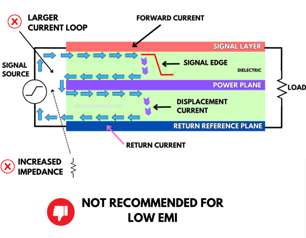
Figure 21 - Return current path when a power plane is used in between signal and return reference layer.
At lower frequencies, coupling capacitors can help by allowing the return current to flow through them. However, this only works for low-frequency signals. For high-frequency signals, the impedance of the capacitors limits their effectiveness. At higher frequencies, the return current depends on the distance between the two planes, which creates impedance between them.
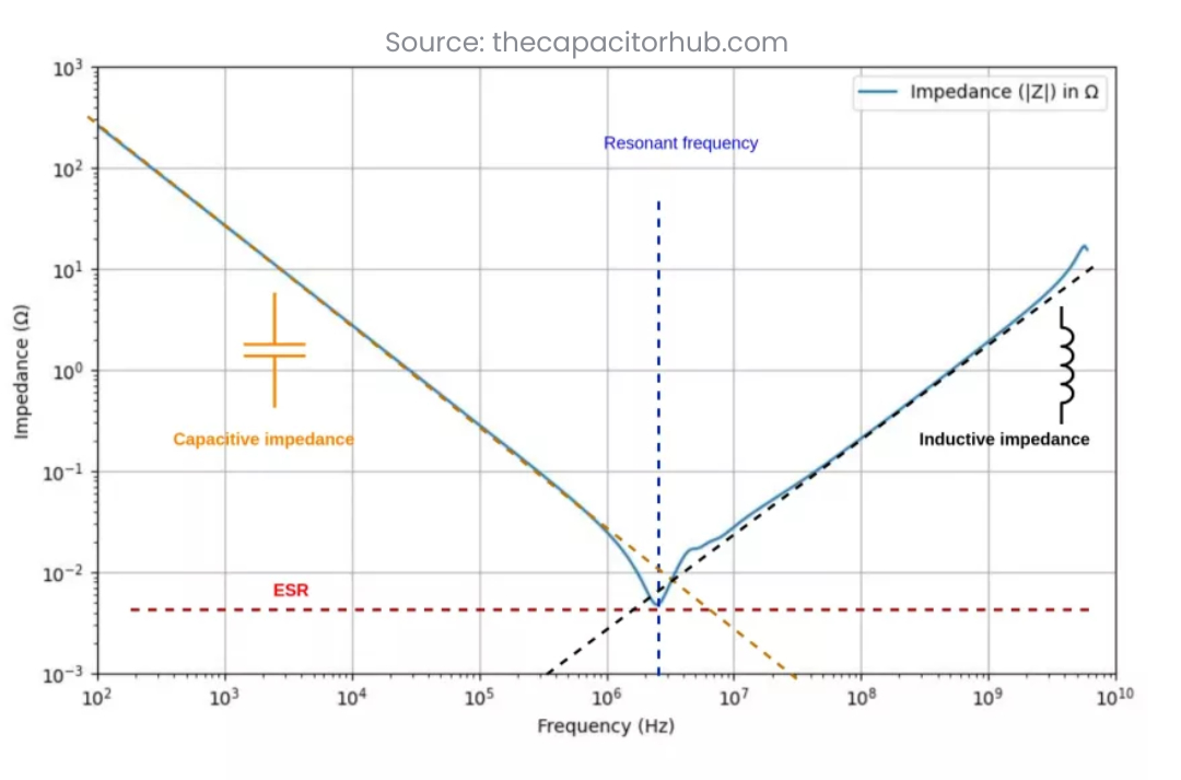
Figure 22 - Real impedance characteristic of the capacitor.
The impedance between the planes is the issue. When the return current crosses from the power plane to the "ground" reference plane, it faces this impedance, causing a voltage drop. This voltage drop creates noise, which can potentially show up in EMC testing. Since the power and return reference planes are not DC electrically connected, the return current must find a way to move from one plane to the other.
This happens through displacement current, but its path is unpredictable and will follow the path of least impedance, which may not be ideal. Relying on the power plane as a return reference is risky because it introduces uncertainty and can lead to difficult-to-manage problems.
It’s best to avoid using the power plane as the return plane due to the risks and potential problems it may cause. Other lesson explor this concept further so we will not dwelve deeper into this topic here. The best approach is to use a dedicated return reference plane, typically the "GND" plane. For each signal layer, having an adjacent return reference plane ensures a clear and consistent path for the return current, which helps maintain signal integrity and reduce noise.
Layer 6
This layer presents similar issues as the first layer.
The major issue here is the lack of a full return reference plane adjacent to it on layer 5.
As we have seen in this lesson, this will create impedance discontinuities that are not only important in terms of signal integrity, but also even more important in terms of EMI.
Figure 23 - Layer 6 of the PCB.
The most important fact is that by providing a solid return and reference plane on layer 5 for the signal on layer 6, we avoid the creation of a common mode voltage source, which will drive common mode currents that are very effective at radiating emissions.
The second major improvement for these layers is to remove the copper pours so that the available real estate on the board can be used efficiently, maximizing the distance between the traces and reducing signal crosstalk.
Obviously, this optimization comes second to the need for having a solid return and reference plane on layer 5.
Conclusions
The video lesson dives deeper into the nuances of the project and can do a better job of explaining certain topics that are harder to explain in a text format. Nonetheless, the topics covered in this lesson are already discussed in much greater detail in other lessons. Therefore, the scope of this lesson was to show the application of those core fundamentals in a real-world application.
At fresuelectronics.com, our primary goal is to help you circumvent the pain associated with this steep learning curve. We believe that by sharing this guide, along with the courses, materials, and programs we offer, we can assist you in navigating the complexities of PCB design.
Our aim is to support you on your path to mastering this field, ensuring that you have the tools and knowledge necessary to succeed.
If you would like to master EMC/EMI design, we have a new training program here:
There, you’ll find details on how to apply for one of our exclusive programs designed to help you achieve that goal.