

Action list:
1. Get the New EMI Quick Fixes Guide - 2025
In this lesson, we’ll review an MPPT project for solar panel applications, focusing on EMC (Electromagnetic Compatibility) and signal integrity. I’ll highlight some common mistakes that you’re likely to encounter more frequently when reviewing PCBs for low EMI. We’ll also explore techniques that can help improve the project’s performance in these areas.
Stackup Analysis
When reviewing any project for EMI (Electromagnetic Interference), the first thing I would usually look at, is the board's stack-up. This is a key factor in the success of the project. The stack-up is particularly important because it affects around 90% of the project's EMC performance. Looking at the stack-up, we see it's a two-layer design. With signals placed on both the top and bottom layers, we can already anticipate potential issues. The main concern is the lack of a dedicated reference plane for the signal return paths, which can lead to EMC problems.
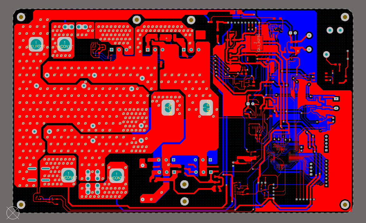
Figure 1 - MPPT Project under review
What Do We Mean by Return Reference Plane (RRP)?
A return reference plane (RRP) refers to a return plane that is adjacent to the signal traces. This is important because it provides the reference for the signal's voltage but also the path for the return current.
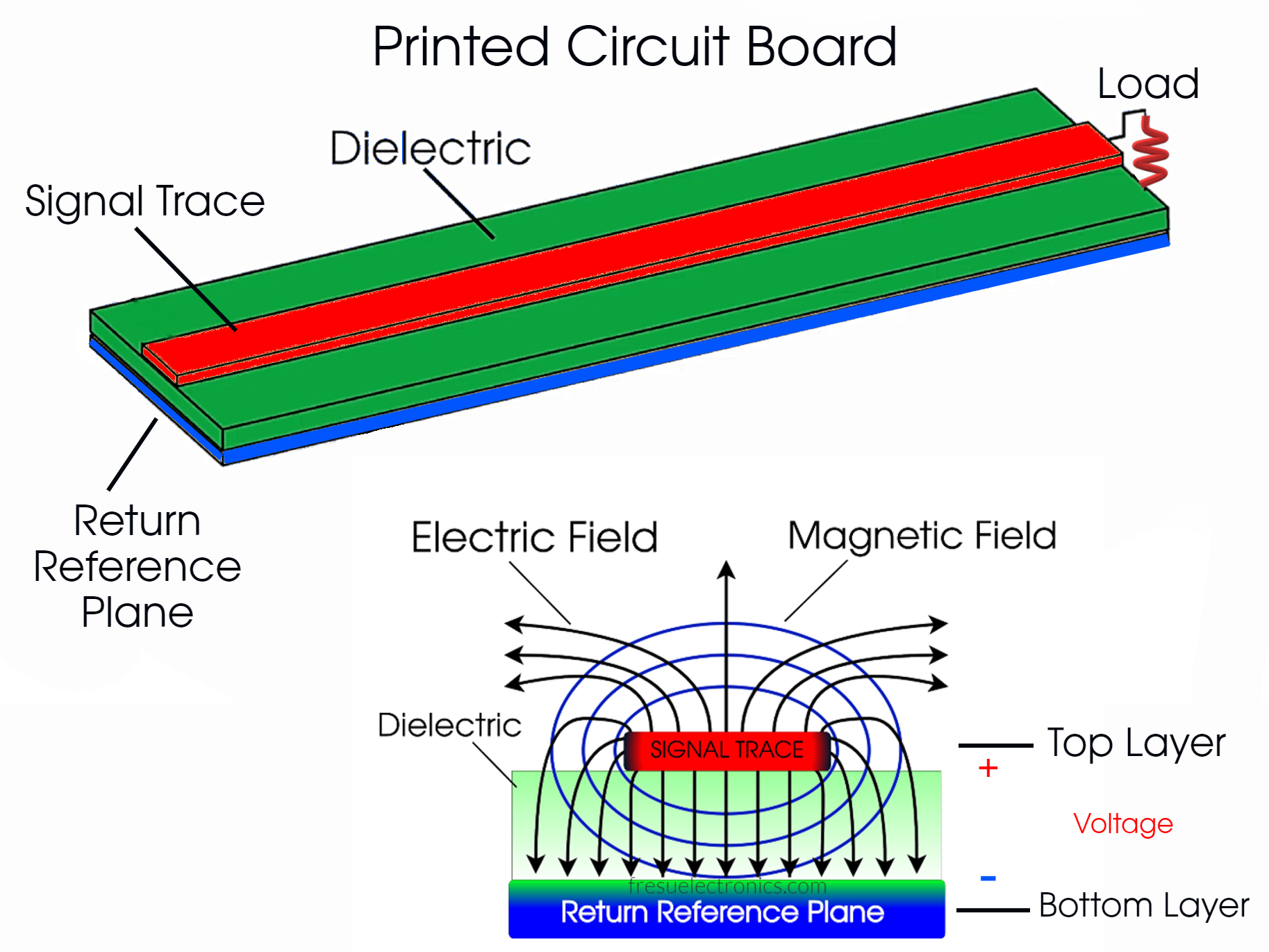
Figure 2 - Electromagnetic Fields in a PCB
The reference plane also plays a major role in containing electromagnetic fields. Without it, the fields can spread out uncontrollably. In this project we are reviewing, there is no return reference plane underneath the signal traces, which will cause the fields to spread.
Another issue arises when there are two signal layers, such as signals on the top and bottom layers, as in this design. What happens here is that the fields from the top signal trace can interfere with the fields from the bottom signal trace, and vice versa.
This creates crosstalk, where signals from one trace are "seen" by the other trace. In simple terms, the fields from the top trace contaminate the fields of the bottom trace, and vice versa. When this happens, the signal on the top layer can affect the signal on the bottom layer, leading to unwanted interference.
Consider an example where you have a trace for a reset line and an adjacent trace for an interrupt signal. Let’s suppose you want to measure when the temperature rises above a certain level. The interrupt signal on the bottom trace is responsible for detecting this temperature rise. Meanwhile, the reset line on the top trace is used to reset your microcontroller or CPU.
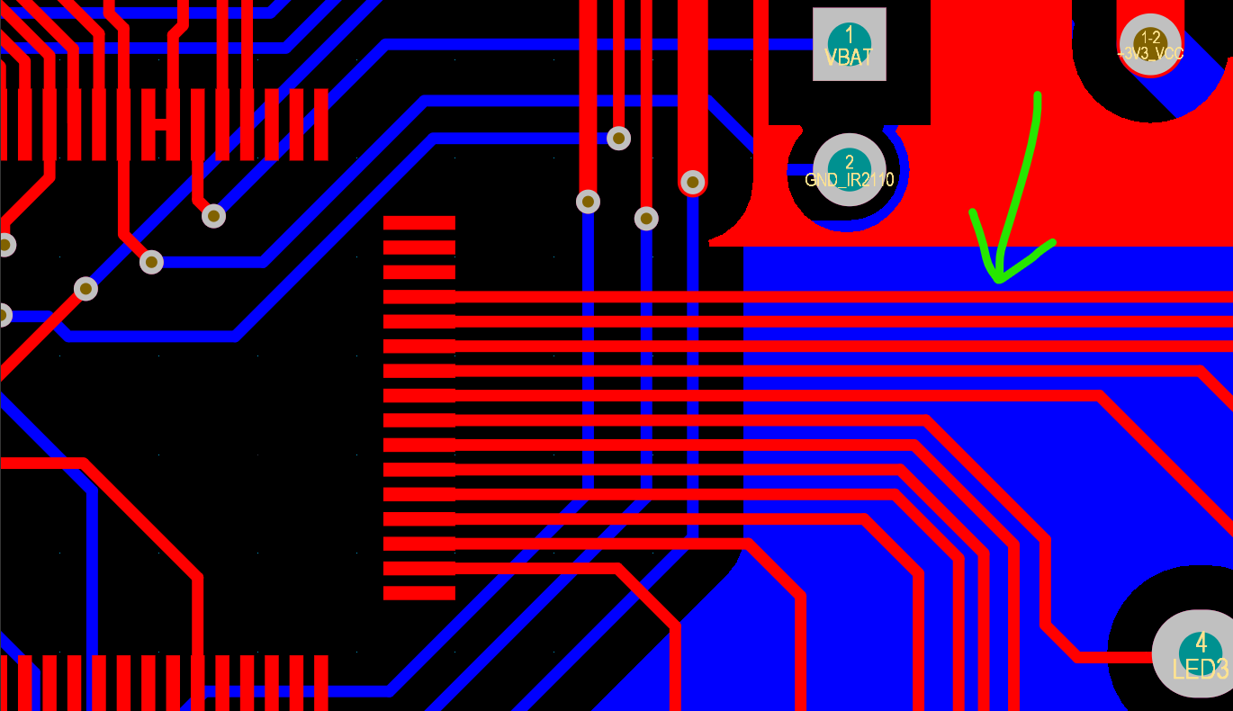
Figure 3 - Example of signal traces routed too close to each other.
Here’s the issue: When the interrupt signal triggers, let’s say the temperature reaches 37°C, the CPU is supposed to take certain actions. The interrupt should notify the CPU to perform specific tasks. However, the reset signal, being on the top trace, also detects the high logic voltage level of the interrupt signal on the bottom trace. As a result, the CPU mistakenly interprets this as a reset request. Instead of responding to the interrupt, the CPU resets itself, because it thinks a reset has been triggered. This can lead to catastrophic failure, depending on the system and the actions required by the interrupt signal.
We want to ensure that the signal is contained within the dielectric in bewteen its conductor traces and that it is not contaminated by other signals. To achieve this, we need to ensure the fields are contained properly, which requires having a return reference plane that manages these fields.
If you look at the electric field lines in Figure #, you'll notice that from the top, they tend to spread outside the board. The fields are on the bottom instead are contained within the dielectric material between the two layers, and they are referenced and contained by the return reference plane.
A two-layer board presents challenges because, in such a design, you can either have the signal on the top, and the return reference plane on the bottom, or vice versa. However, using two signal layers introduces a significant problem. In this case, with signals on both the top and bottom layers, the fields from each layer interfere with each other, creating unwanted noise and crosstalk. This is also why, to fix this, we typically use a four-layer board.
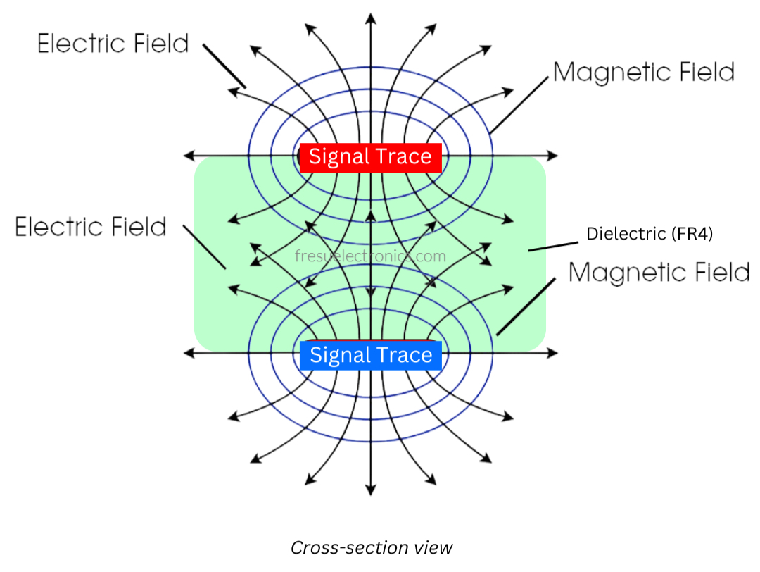
Figure 4 - Example of electromagnetic fields interfering with each other.
So it should be clear at this point that we need to increase the number of layers. I've also explained in other videos why we don't want a dedicated power layer in a four-layer stack-up when two layers are already dedicated to signals. But instead, it's preferable to have an additional GND layer to act as a return reference plane. As a side note, while we commonly call this layer "GND," it's more accurate to refer to it as a "return reference plane" (RRP) to avoid confusion. So, here we will call it RRP for the return reference plane.
Before proceeding, the action needed at this point is to change the layer stackup into the following:
- Layer 1 - Signals/Power
- Layer 2 - Return Reference Plane
- Layer 3 - Return Reference Plane
- Layer 4 - Signals/Power
For the Return Reference Planes, I will also add solid (no splits or cuts) copper planes, which will act as the return reference plane.
Layout Analysys
Now, let's take a closer look at the layout. Since we didn't have a return reference plane, but we had the ground net, GND IR 2110, this was previously implemented as traces. Now that we have a return reference plane on the second and third layer, adjacent to the signals, we can remove these GND traces and the copper fills on the signal layers.
Why is this important?
Earlier, with just two signal layers, there was a significant distance between the signals and their reference traces (GND IR 2110). This was a large impedance gap. However, by switching to a four-layer design, the distance between the signal and return reference plane has been reduced. This is important because it provides much better coupling between the signal on the top layer and the return reference plane on the second layer, and the same applies between the signal layer on the bottom, and the RRP on the third layer. Additionally, reducing the distance between signals and return reference layers is one of the most effective ways we have to also minimize crosstalk.
Antenna-like Structures
Next, let's focus on avoiding ground pours that create antenna-like structures, like the one shown in Figure #. This ground pour has an antenna-like design, for instance like a dipole antenna-like structure.
A dipole consists of a signal source with one side having a certain voltage and the other side having the opposite voltage. This configuration acts as a good radiator, which is undesirable. We don't want structures that form this kind of antenna.
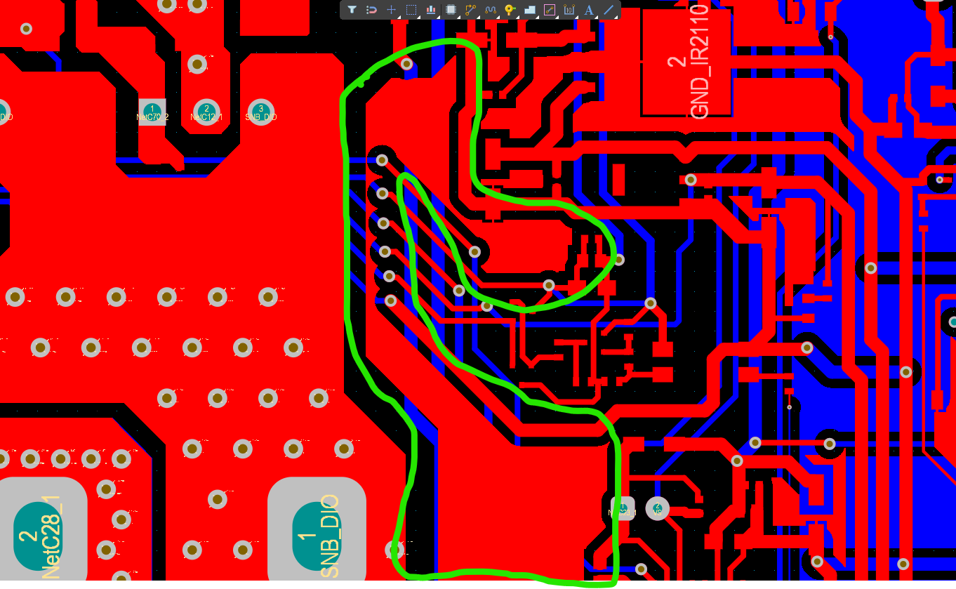
Figure 5 - Example of antenna-like structure.
This issue is similar to placing a cable on one side of the board and another cable on the opposite side. This creates a dipole antenna, which can radiate or receive electromagnetic interference, both of which are undesirable. We should avoid creating these antenna-like structures because they promote radiation.
When the signal from the trace reaches this area near the polygon, it forms a dipole and promotes radiation. Therefore, it's best not to use this type of polygon pour.
The same applies to Figure #, where another antenna-like structure exists. The copper has a specific impedance in between points, and this results in a voltage difference, which in turns creates a dipole. Again, we want to avoid such geometries.
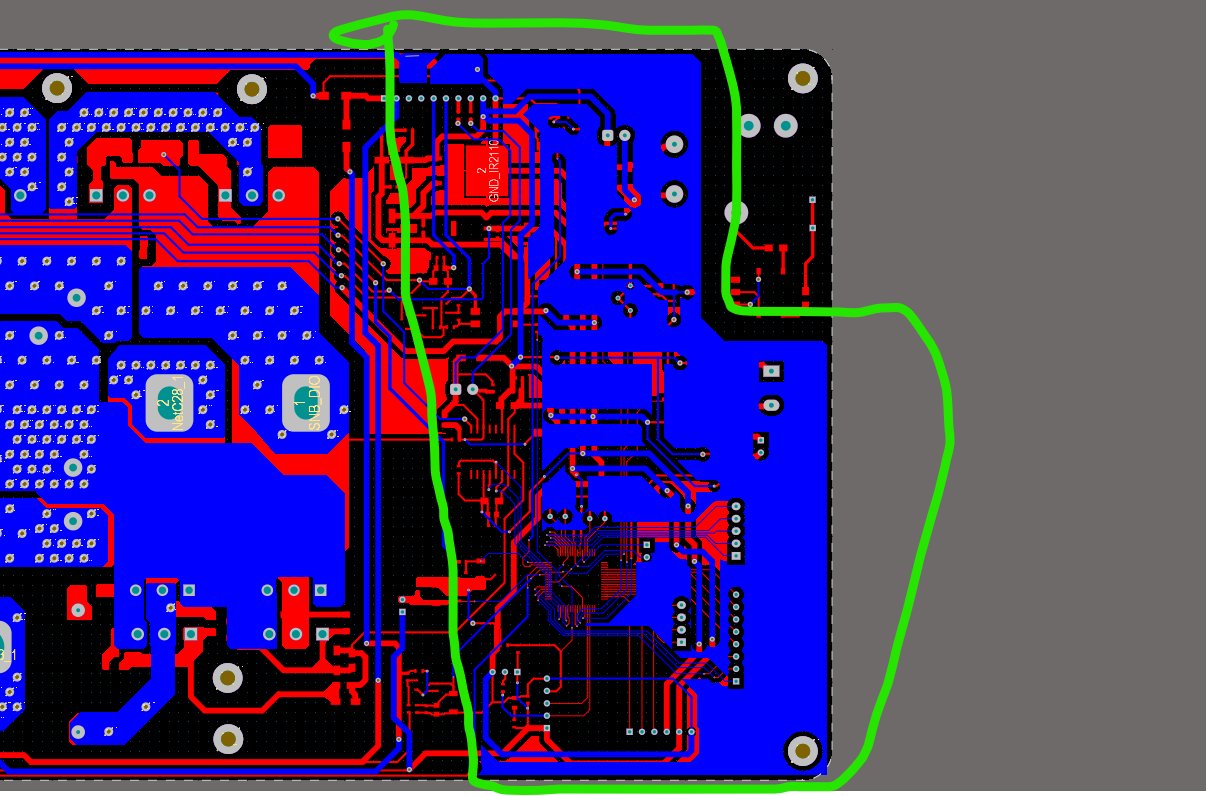
Figure 6 - Another example of antenna-like structure.
To fix this, we’ll remove the structures that form these antenna-like shapes. Once we do that, the design will also start to look cleaner.
Similarly, we’ll address the issue in the next section by removing these undesired structures. This will leave us with some unconnected nets, but that's okay, we’ll fix that in the next steps.
💡 By the way, If you would like to master EMC/EMI design, we have a new training program here:
There, you’ll find details on how to apply for one of our exclusive programs designed to help you achieve that goal.
Improving the Layout
There are many traces here that can be cleaned up, which will also help reduce their inductance. Currently, these pads in Figure # are contributing to inductance in the circuit.
You can see that a trace connects the pads, but this adds inductance because the trace itself has some inherent inductance.
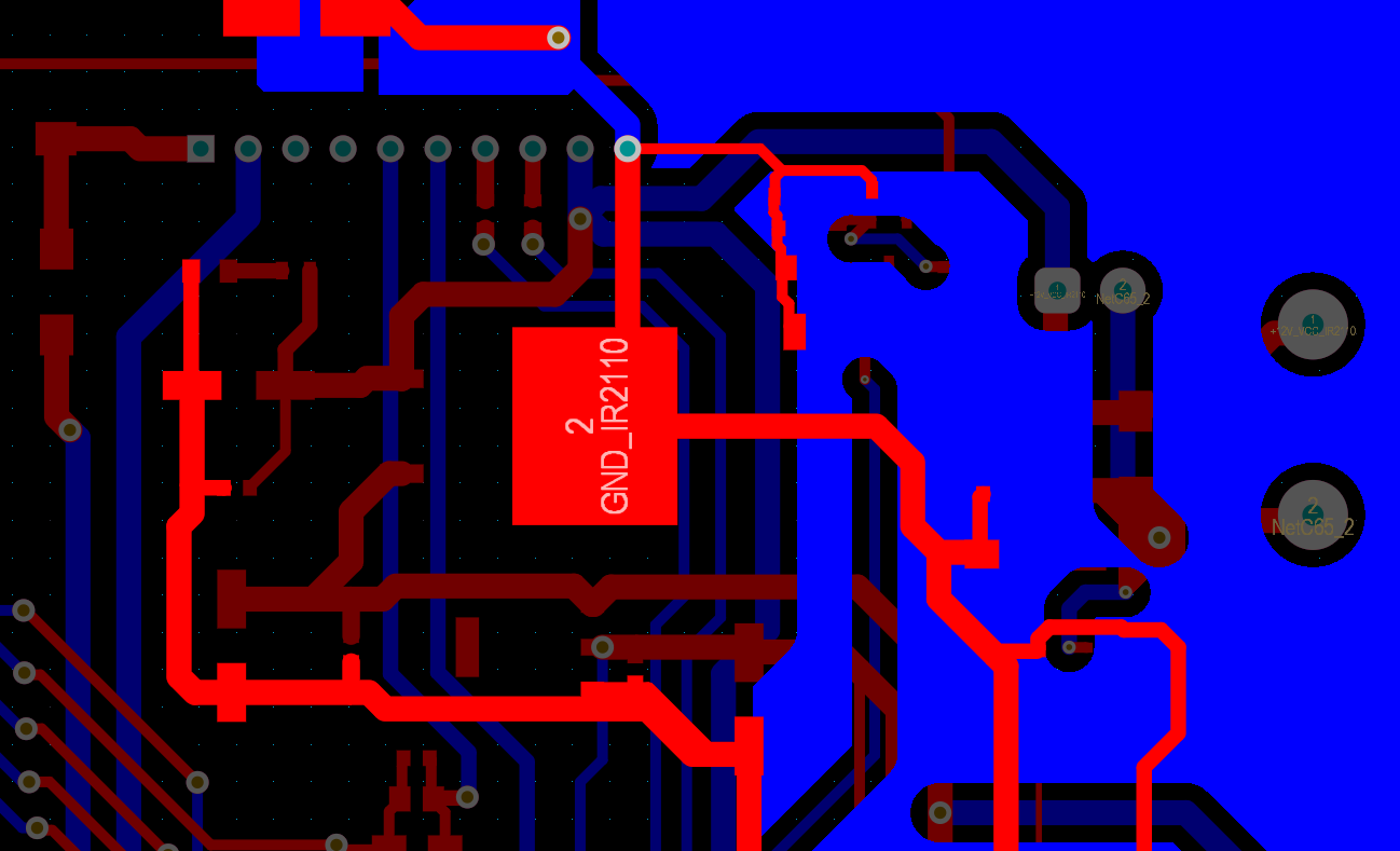
Figure 7 - High inductive paths in the GND net.
Since we now have a return reference plane on the second and third layers, here's what we can do:
First, we'll place the via as close as possible to the components' pads. After that, we’ll adjust the trace width. we can use a width of 0.8 for now, but we need to calculate the ideal trace width based on the impedance we require, especially for signal traces. I can use tools like Saturn PCB to calculate the width based on the required impedance and the current load.
Once the width is calculated, we’ll choose the layers we want to connect to. In this case, we want to connect the RRP net. We’ll place the via in the middle and add the via connection. By reducing the distance between the components and connecting them directly to the return reference plane, We’ve created a path with very low impedance, improving signal integrity.
What we are doing here is reducing the current loop size for these nets. Now, we are going to apply the same process to the other parts of the layout. We’ll start by selecting all the GND traces, and then we'll remove them. Next, we’ll replace these traces with vias that directly connect to the return reference plane. We’ll do the same for all other traces: select them, delete them, and begin cleaning up the layout. We’ll continue to remove these unnecessary connections. By the end of this process, none of these traces will remain.
This cleanup process helps remove elements that aren't necessary, making the layout much cleaner and efficient by reducing extra impedance. At worst, these leftover traces could just contribute parasitic effects.
If we leave these traces, they will create parasitic loops, which can increase the current loop size and, in turn, increase the radiated electromagnetic fields due to the generation of common-mode currents. The larger the current loop, the larger the fields, which is something we want to avoid. This is actually one of the most common problems you'll encounter during EMC tests.
Improving Vias' Current Capabilities
For trace paths that require a significant amount of current, you need to calculate how much current can safely pass through the via. For example, this via has a hole size of 0.3 millimeters and a diameter of 0.6 millimeters. You can perform a quick calculation, for example with Saturn PCB to determine the current capacity.
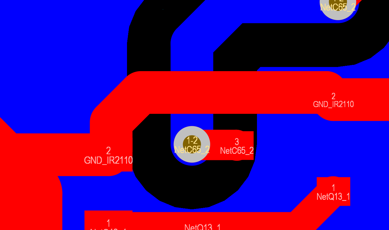
Figure 8 - Example of signal via.
Given the 0.3 mm hole size and 0.6 mm diameter, along with the default plating thickness, this via can carry approximately 2.16 amps. If you need to handle more current, you can either increase the number of layers or increase the size of the via. You'll need to calculate these adjustments based on your specific requirements.
Signal Crosstalk
The next thing we need to address is crosstalk, which is very important. It is often possbile to identify potential issues just by examining the distance between the nets. For example, when we look at these nets, we can see right away that they’re not differential pairs. If I have any doubt, I can check the schematic, but we know that the SWDIO connection is not a differential pair. Looking closely at these traces, we notice that they are very close to each other, just 0.25 millimeters apart, which is about the width of the signal trace, therefore far too close.
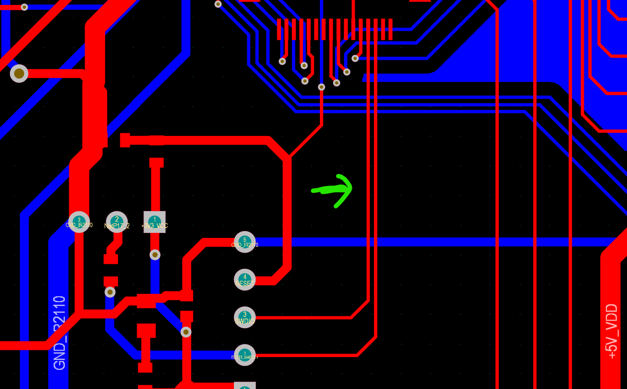
Figure 9 - Example of signals routed too close together.
This means the clock signal from one of these nets will likely affect the SWDIO net. To reduce crosstalk between these traces, we can increase the distance between them. By spacing the traces at least two or three times the width of the net, as a general rule of thumb, we can significantly reduce crosstalk.
Since we’ve reduced the distance between the signal layer and return reference plane now very close to each other, I know that crosstalk will be minimal. If I have any doubts, I can always double-check even with tools that offer a free crosstalk calculator.
It's important to note that some signals can be triggered by very low voltages. For example, certain MCUs or CPUs have low threshold voltages for detecting high logic level signals. If the crosstalk is high enough, it could cause the system to mistakenly detect a high signal when none was intended. This is one of the kind of issue we want to avoid. So, to minimize this risk, we increase the distance between the traces.
Of course, as already mentioned, you’ll want to improve these traces to improve the crosstalk and the EMI behaviour, however, you also want to make them more refined and visually appealing. A good layout isn't just about performance; it’s also about aesthetics. Your clients will see your layout, and they will judge it based not only on its functionality but also on its appearance.
Signals too close to the edge
Next, let's focus on the traces near the edge. Ideally, you want to position them further from the edge to avoid fringe fields, which are essentially fields that extend outside the board.
Figure 10 - Example of signals routed too close to the board edge.
By keeping the signal trace further inside the board, the fringe fields can better reference the return plane adjacent to the trace. If the fields extend outside the board, they are not contained, which can show up during EMC testing. So, we are going to move the traces inward, and also shorten their length to reduce this risk.
Stubs
Moving to the next issue, here we have what are called stubs. You want to avoid creating these types of branches. What happens here is that the signal, whether it’s coming from one direction or another, reaches the branching point and encounters these two branches. This is called an impedance discontinuity.
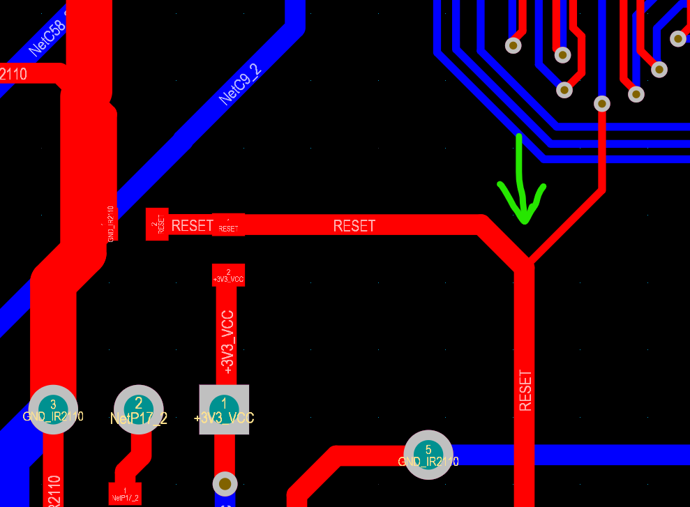
Figure 11 - Example of stubs (branches).
For example, if the impedance here is 50 ohms, the signal will split when it reaches the branching point because the impedance changes. This mismatch in impedance causes reflections, which can lead to signal integrity issues. Therefore, you should avoid creating branches like this.
To fix this, we should create point-to-point connections. Instead of branching off here, we continue the connection from pad to pad. In this way the signal no longer splits. It flows in one direction, without encountering any impedance changes. The key is to ensure that the signal sees minimal impedance mismatch as it propagate through the design.
If this is a power trace, this branching is less importnat, you may also want a wider trace, sized, of course, according to the current requirements. However, for a signal trace, it's important to maintain a controlled impedance, typically 50 ohms for regular signals, until it connects to the pin.
Ground Bounce
Now, let's take a look at one of the biggest issues this board had: ground bounce. The problem, in this case, stems from impedance discontinuities in the return path.
When two signals share the same return path, like the ground traces we saw earlier, there’s a higher likelihood that they’ll both use the same low-impedance path. As a result, when one signal triggers, the other may also trigger because they are coupled together. In this case, for example, the signal from the bottom layer causes ground bounce because both signals likely share the same return path, leading to interference.
This issue can occur in both the signal path and the return path. When it happens in the return path, it's referred to as ground bounce. To resolve this, we can either increase the distance between the signals, or reduce the distance between the signal path and the return reference path. By doing so, we ensure that the fields are more tightly contained, preventing interference between them.
Large Current Loops
Let's look at the buck converter circuit. It includes an inductor that interacts with the system’s magnetic fields, along with a filter composed of inductors and capacitors. The current loop formed by these components is crucial to manage.
Figure 12 - Example of the large current loop in the buck converter.
When a switching current flows through the circuit, it generates changing magnetic fields. These fields can interfere with other traces and devices on the board. During EMC (electromagnetic compatibility) testing, these fields may exceed limits and cause failures.
🔓 Our goal is to minimize the size of the current loop.
It starts at the input, passes through the fuse, feeds the buck converter, and then closes the loop through the inductor and capacitors. A large current loop is problematic because the changing magnetic fields it generates can be detected during EMC testing, leading to failure.
The solution is to minimize the loop's size, ensuring the current follows the shortest, least-impedance path. Initially, a large copper pour connected to the capacitors created a large, poorly optimized loop. By connecting directly to the capacitors, we shorten the return path and reduce the loop size.
This adjustment improves the return current path, reducing magnetic fields and minimizing the loop's size. The new design after this revision will use full return reference planes, allowing the current to follow the path of least impedance. This also shortens signal paths, reducing potential electromagnetic interference.
It's important to remeber that, the type of signal and its involved frequencies, affects the return current's behavior. For high-speed signals, the return current flows directly beneath the signal trace, minimizing inductance. For low-speed signals, the resistive path becomes more important, and the return current takes the shortest route back to the source. Also a quick tip here is that if we want to minimize large current loops, components like capacitors should be placed as close to the pins they are feeding or filtering.
Component Placement
When placing components, it’s crucial to maintain proper separation, especially based on the type of circuitry they belong to. For example, components should be grouped into distinct sections, such as a digital section and an analog section, while avoiding the splitting of planes.
🔓 We avoid splitting the return and reference planes (also known as "grounds"), even though some application notes might recommend doing so.
Instead of separating the analog and digital sections within the return reference plane, we place them apart from each other on the signal layers, providing enough distance to prevent unwanted coupling. This separation is achieved by placing components at a distance, not by cutting or splitting the planes.
We do not cut planes or create segmented regions within the planes. Solid copper planes should be used, with no splits or cuts for either the analog or digital planes.
Stitching Vias
Another common issue is managing the transition of signals from one layer to another, such as when a signal moves from the top layer to the bottom layer. The problem occurs during this transition because, as the signal moves downward, there is no longer a return reference plane in the immediate vicinity. This results in uncontained fields, which can lead to electromagnetic interference.
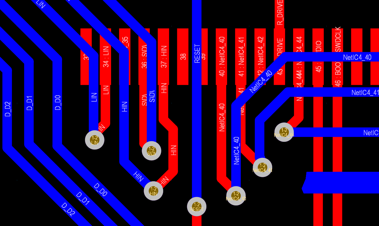
Figure 13 - Example of signal vias without stitching vias next to each other.
When the signal transitions from one layer to another, the fields are no longer contained. This causes the fields to spread out, and if the levels are too high, will lead to failure during the electromagnetic compatibility (EMC) tests. To prevent this, we add at least a return via next to the signal trace at the transition point, or as in the case below four return reference vias. This ensures the signal has a 360 degree reference and that the fields remain contained even during the vertical propagation of the signal.
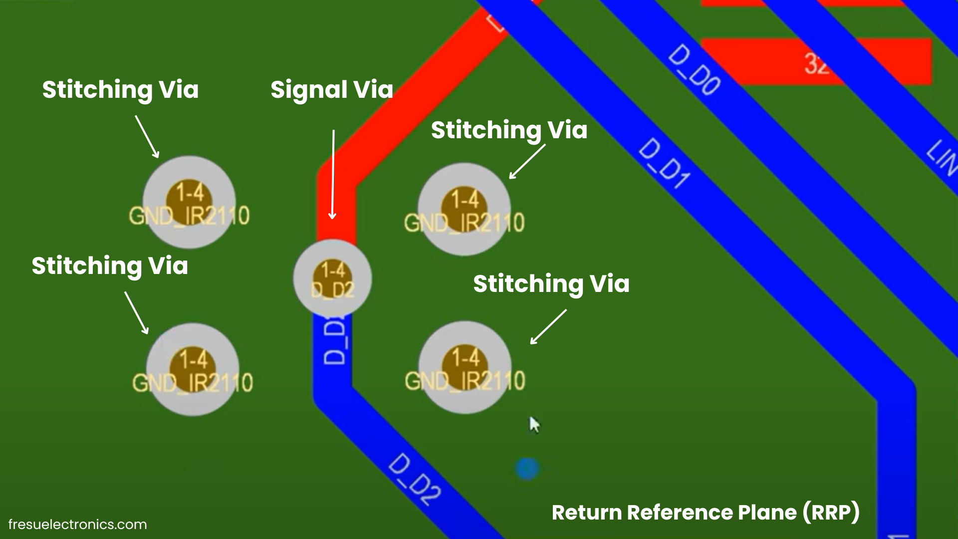
Figure 14 - Example of stitching vias to support the transitions of the signals across layers.
With return vias added, the signal transitions smoothly to the bottom layer and finds a return path, ensuring minimal field spread. This approach reduces current loop size, keeping it short as the signal crosses layers. Once the signal reaches the other side, it continues to propagate without any electromagnetic interference problems. Wherever there’s a layer transition, place return vias to ensure proper reference and minimal signal interference.
Another important step to consider is the impedance in between planes of the same voltage, such as the return reference planes. As we discussed, copper planes (and traces) are not ideal and have a certain resistance and impedance. Between two points on these planes, there is an impedance that causes a voltage drop when current flows through it.
To minimize this voltage drop, we need to make these planes equipotential. The way to achieve this is by adding stitching vias across the planes. To determine where to place these vias, you should select a grid appropriate for the fastest signal on the board.
If the distance between the vias is too large, you create a cavity between the planes, which may resonate at a particular frequency within your frequency of interest. This cavity is defined by the distance between the two points where the vias are placed.
To calculate this, first, determine the wavelength of the fastest signal, in the dielectric material (such as FR4). You should focus on the wavelength within the material, not in the air. Once you have this, measure one-tenth of the wavelength to find the appropriate distance between the stitching vias.
For example, if the one-tenth wavelength of the signal in the dielectric material is 2.5 mm or higher, you should place stitching vias at this distance. You can either manually place the vias or use the CAD tool which may have features to automatically add stitching vias.
By placing the vias in this manner, the multiple return and reference planes will be coupled, and their potential will become uniform across the entire planes. This help eliminate the issue of voltage drops caused by impedance between the two points, which could otherwise induce noise that could couple with other traces.
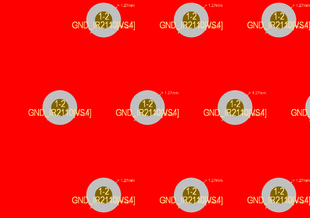
Figure 15 - Example of stitching vias arranged in a grid-like pattern.
However, a downside to adding a large number of stitching vias is that it can increase the manufacturing cost of the board due to additional drilling requirements. To ensure the cost stays within budget, you should check with your PCB manufacturer for their drilling cost guidelines. This information is typically available in their capabilities documentation, under the section for drilling costs.
By adding stitching vias, you ensure that the planes behave like the return vias used during signal transitions. This solves many potential issues, as the stitching vias will effectively serve the same purpose as placing return vias next to signal traces. Even without explicitly adding return vias next to every signal, placing stitching vias improves the likelihood that the return current will have a clear path, minimizing potential issues.
What if I cannot add more layers to the stackup?
For those of you whose managers insist on using a two-layer board instead of a four-layer board to reduce costs, the first step is to assess if this is feasible. You need to consider whether it is possible to route all the traces on one side of the board, so the other side can be used as the return reference plane.
If you plan to make voltage layer transitions (for example, from a top layer to a bottom layer), the key is to keep these transitions as short as possible. For instance, the signal can go from the top layer to the bottom layer, and then return to the top layer before continuing along the top layer. This approach minimizes the length of the trace on the bottom layer.. The goal is to maintain short, direct paths for both the signal and return currents.
To ensure the trace width is consistent across the transition, the width on the top layer should ideally remain the same. For example, if the trace is 0.24 mm wide, the transition to the bottom layer should preserve this width as much as possible, before returning to the top layer and continuing along the signal path.
By minimizing the cuts on the bottom layer, and making them as small as possible, you’ll avoid significant interference with the return current. If you use the bottom layer as the return reference plane, these short trace transitions will not cause major problems.
🔓 In some cases, it’s still possible to route the board as a two-layer design, but it’s important to figure out how to place all the traces on one layer while using the other as the return reference plane.
You can either place all traces on the top layer and use the bottom layer as the reference plane, or place all traces on the bottom layer with the top layer as the reference plane.
One critical consideration is ensuring the power ratings of the traces and planes are sufficient to handle the required current. For instance, if the board needs to carry 50 amps of current, you need to calculate whether the copper traces can handle this load. If not, you may need to increase the size of the copper traces to support the current.
Additionally, when using a two-layer stack-up, be mindful of the voltage ratings. If high voltage is involved, ensure that the clearance and creepage distances meet the safety standards. For example, if you have high voltage traces on the bottom layer and use the top layer as the return reference plane, verify that the dielectric material between the layers provides adequate insulation according to the required safety standards.
Conclusions
I hope this project review is helpful and enables you to pass EMC testing more easily. There are still a few things we haven't addressed yet, such as checking and providing protection for input and output cables, or any connections extending outside the board. It's important to include protection, such as TVS diodes, filtering, and other essential components. Adding these protections will enhance your board's immunity to EMI and reduce the EMI it generates. These are some of the basic considerations we look for in a design review. As demonstrated in this review, it's quite simple to improve your layout significantly, starting by the PCB stackup, and in certain cases simply by adding two more layers.
At fresuelectronics.com , our primary goal is to help you circumvent the pain associated with the EMI steep learning curve. We believe that by sharing this guide, along with the courses, materials, and programs we offer, we can assist you in navigating the complexities of PCB design. Our aim is to support you on your path to mastering this field, ensuring that you have the tools and knowledge necessary to succeed.
If you would like to master EMC/EMI design, we have a new training program here:
There, you’ll find details on how to apply for one of our exclusive programs designed to help you achieve that goal.