The first decision you make on a new board — the layer sequence — determines most of your EMC and signal integrity outcome. Here's why using power planes as return paths is one of the most common and costly mistakes in the stack.

A typical 4-layer board might look like this: signal top, power plane, return reference plane, signal bottom. It seems logical — power distribution is handled by a dedicated plane, signals run on the outer layers. In practice, this configuration creates serious problems that only become visible at EMC testing.
The reason comes down to how return current actually behaves — which is not how most engineers expect it to.
At low frequencies, return current takes the path of least resistance — the shortest route back to the source. But even at a few kilohertz, inductance begins to dominate. The return current starts concentrating directly beneath the signal trace, following the path of least impedance. At high frequencies — the range where EMC problems live — this concentration becomes very tight. The return current hugs the signal trace from directly below, minimising loop area and containing the electromagnetic field.
This is not a design choice. It is a physical consequence of how fields minimize energy. The board designer's job is to ensure the return current has a clean, uninterrupted path directly beneath every signal — and that means placing a solid return reference plane adjacent to every signal layer.
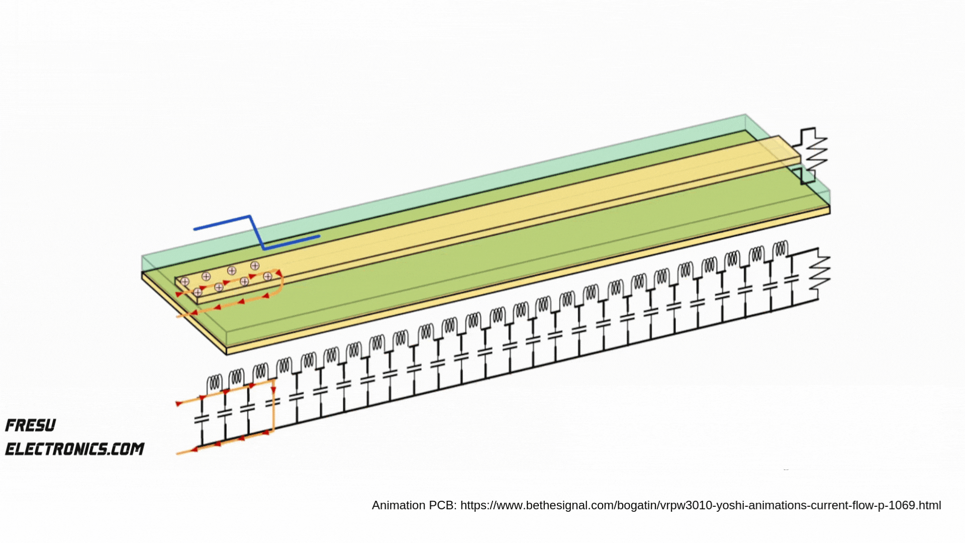
Diagram illustrating the signal and current flow through a PCB layer.
Return current doesn't ask permission. It will find a path — the question is whether that path is the one you designed or one you didn't.
A power plane carries DC supply voltage with superimposed switching noise. When a high-speed signal on the top layer references a power plane instead of a ground plane, its return current must travel through the interplane capacitance between the power and ground planes before it can close the loop. This introduces impedance discontinuities, creates common-mode noise on the power distribution network, and forces the return current through a path that was never designed for signal integrity.
The result: larger effective loop areas, increased radiation, and coupling paths between signals that share the same power plane reference.
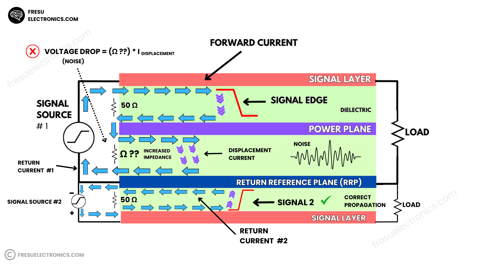
Diagram illustrating signal and current flow in a multi-layer PCB, highlighting the effects of impedance and noise across signal layers, power planes, and return reference planes for proper signal propagation.
A common counterargument is that interplane capacitance between power and ground planes provides a low-impedance return path at high frequencies. This is partially true: tightly spaced power/ground plane pairs do create useful distributed capacitance. But this capacitance is effective for power distribution noise decoupling — not for signal return. The inductance of the path from a signal trace through interplane capacitance and back is significantly higher than a direct return through an adjacent ground plane. At the frequencies that matter for EMC, the difference is significant.
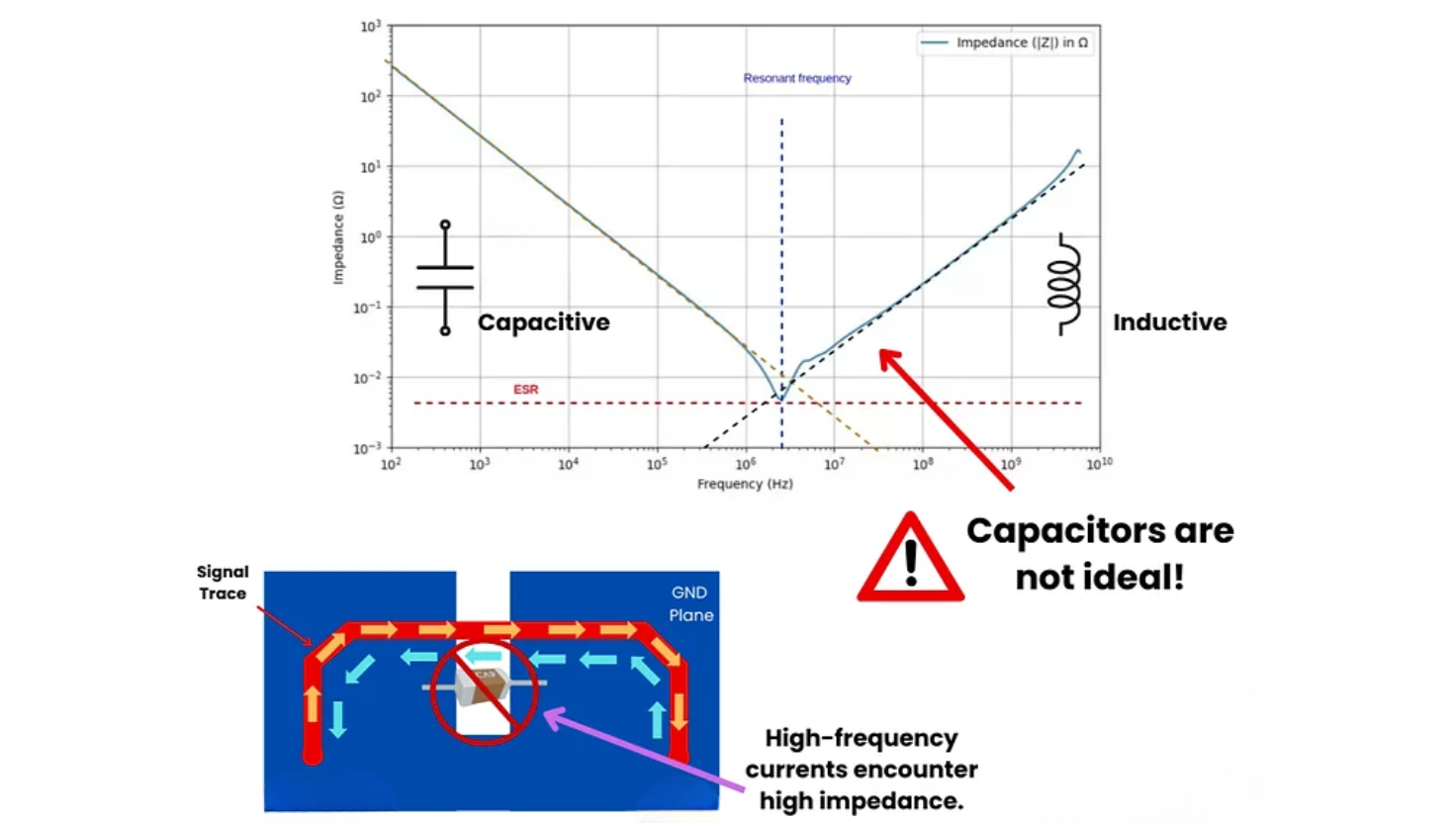
Graph illustrating the impedance characteristics of capacitors, showing a transition from capacitive to inductive behavior at the resonant frequency.
The return reference plane must be immediately above or below the signal layer — not separated by another layer. Every additional layer between the signal and its return plane increases the loop area and the radiated emissions. The tighter the coupling, the smaller the field, the cleaner the board.
Any cut or split in the return reference plane forces return current to detour around it. The detour creates a large loop — effectively an antenna. This is one of the most common causes of a clean-looking board failing EMC. The ground plane must be continuous under every critical signal trace.
When a signal changes layers through a via, its return current must also change layers. Without a nearby return via, the current must travel laterally across the plane to find a stitching via — creating a loop. Always place a return via adjacent to every signal via, especially for high-speed or high-current signals.
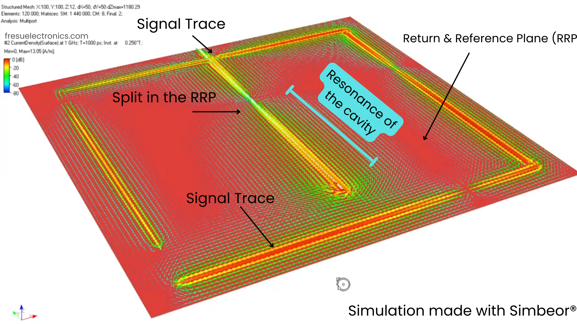
Simulation of a circuit board showing signal trace paths and the return reference plane, illustrating the resonance of the cavity using Simbeor software.
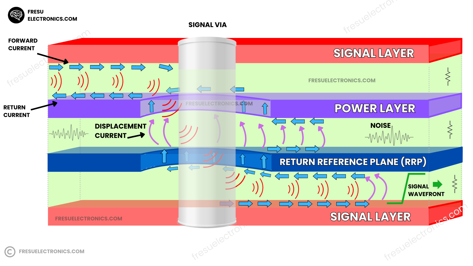
Cross-sectional illustration of a PCB showing signal and power layers with direction of forward and return currents through a signal via, highlighting displacement current and potential noise within the return reference plane (RRP).
For a 4-layer board, the strongest stackup for EMC and signal integrity is: signal — ground — ground — signal. Both outer signal layers reference an adjacent ground plane directly. The two inner ground planes can be tied together at multiple points. Power distribution is handled through the outer signal layers with local decoupling, or on a thin inner layer kept close to a ground plane.
For 6-layer designs, adding a dedicated power plane between the two ground planes gives you PDN performance without compromising signal return paths. The key invariant is that every signal layer has an adjacent, solid, continuous ground plane — no exceptions, no compromises.
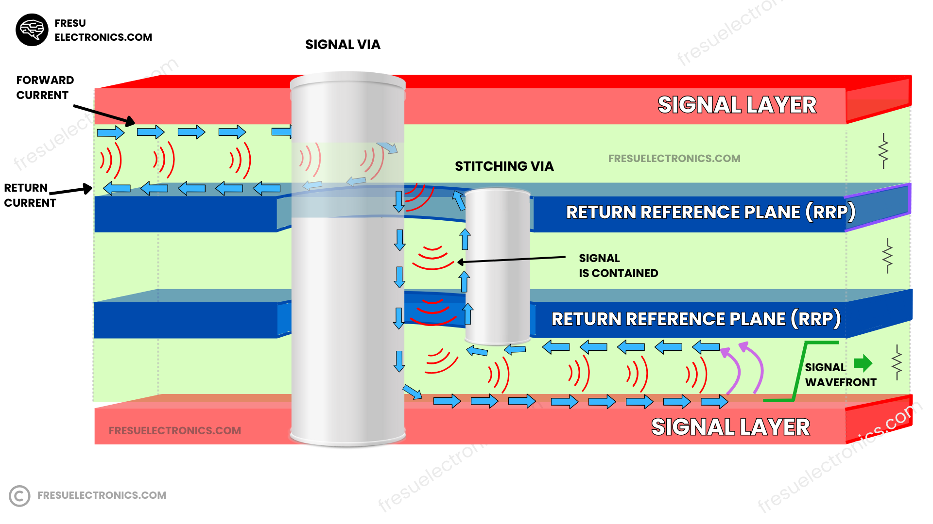
Diagram illustrating signal and return current flow through a PCB, featuring signal and stitching vias, and highlighting the containment of signals within the return reference planes (RRP) to ensure effective transmission.
Work directly with Dario to identify EMC risks at the design stage — before a €15,000–40,000 chamber session reveals issues that require a respin.
Get articles before they're published